An Electrical Model for Multilayered n + /n and Heterostructure Planar Ohmic Contacts
- PDF / 1,635,615 Bytes
- 6 Pages / 414.72 x 648 pts Page_size
- 25 Downloads / 363 Views
Aio
11NTERFACE
S, 10-io *
Ro
METAL CONTACT ; .
•.•.•.. . . . . • . • .• . • . •. . ..
EITXILLAYER Rsk
A
P
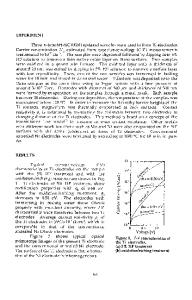
(a) Fig. 1.(a) Two layer metal-semiconductor contact and (b) its standard TLM representation. 443 Mat. Res. Soc. Symp. Proc. Vol. 382 ©1995 Materials Research Society
FET. In this Inpaper, section the 5,TLTLM an example network of is applying used to the model model the non-alloyed to an nq-/n n+/n GaAs contact FET structure of a GaAs is given, showing how when combined with previous contact analyses [4,5], the TLTLM may be used to calculate the parasitic gate-drain resistance and the drain contact resistance.
t/a/
< (•>) :=:'•
io
d
T'
METAL
>
oB
v///////z/z/z/z/z/,
........... "'""'""""
i°(1.•i {'
iof_ • . . . ........ :,:.:.:.:.:.:.:.::::i:i:i:i:
A
sa
u
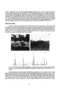
Fig. 2. (a) A three layered n+/n ohmic contact and (b) its TLTLM network representation. 2. THE TRANSMISSION LINE MODEL For planar contacts the contact resistance Rc is taken as the resistance that the device current encounters after passing under the leading edge of the contact as shown in figure l(a). The standard TLM [1] electrically models the contact as a network of distributed resistive elements as illustrated in Fig. l(b). Rsh is the semiconductor sheet resistance (•/[3) outside the contact area while the element Rsk represents the sheet resistance (f2/rq) of the semiconductor layer beneath the contact (a different element value is used as this sheet resistance may differ from Rsh [8]). The element Pc represents the narrow depleted region occurring at the metal-semiconductor interface. The voltage drop beneath the contact in the horizontal direction is attributed solely to the current flow in Rsk while the voltage drop in the vertical direction (perpendicular to the plane of the contact) is due to Pc" The contact has a length d and a width w. 3. MODIFICATIONS TO THE TLM Various modifications have been made to the standard TLM to account for different contact structures and materials. Some of these modifications include (a) As mentioned in section 2, the sheet resistance of the semiconductor epilayer on which the contact is formed has a nominal value of Rsh. Where the contact undergoes an alloying or sintering cycle to make it ohmic, the sheet resistance of the semiconductor layer beneath the contact can alter [2,8]. This modified value is denoted Rsk. (b) The sheet resistance of the top metallization is generally assumed to be zero. In contacts where this cannot be assumed, the electrical network of Fig. 3 replaces the standard TLM network in Fig. 1. Contacts modelled with this network include polysilicon-silicon contacts [4] and silicide-silicon contacts [9]. Here the polysilicon and the silicide are the top contact layers in the respective contacts and have a sheet resistance which cannot be ignored.
444
(c) The TLTLM network is described in more detail in section 4. It allows TLM concepts to be used to model alloyed and heterostructure ohmic contacts where the contact consists of a three layer sequence. The TLTLM model c
Data Loading...


