Barium Strontium Titanate Thin Film Capacitors for Low Inductance Decoupling Applications
- PDF / 365,892 Bytes
- 10 Pages / 595 x 842 pts (A4) Page_size
- 24 Downloads / 366 Views
U15.1.1
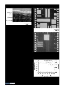
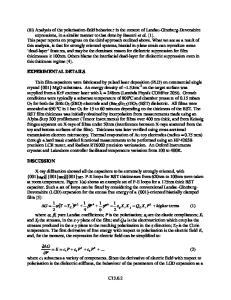
BARIUM STRONTIUM TITANATE THIN FILM CAPACITORS FOR LOW INDUCTANCE DECOUPLING APPLICATIONS J. D. Baniecki, T. Shioga and K. Kurihara Fujitsu Laboratories Ltd. 10-1 Morinosato-Wakamiya, Atsugi 243-0197, Japan ABSTRACT Sputter deposited barium strontium titanate (BST) based thin film capacitors have been developed for use in GHz LSI decoupling applications. The fabricated 1.60x1.85 mm2 BST chip decoupling capacitors with Pt electrodes and 150 µm bump pitch, have a capacitance density of 1.2 µF/cm2, low equivalent series inductance of 15 pH, and a low equivalent series resistance of 0.02 Ω. The impedance of the chip capacitors at 1 GHz is over 1000 times lower than conventional multilayered ceramic capacitors. Fundamental electrical and reliability properties of Pt/BST/Pt thin film capacitor structures were also investigated. Capacitors with 200 nm thick BST thin films deposited at 500 oC by RF magnetron sputtering achieved a C/A of 1.8 µF/cm2, leakage current density < 10-9 A/cm2 at 2 volts, and a breakdown field > 2.5 MV/cm at 20 oC. A fit of the failure data to a Weibull distribution indicated at least two different physical mechanisms causing capacitor failure. The primary failure mechanism for 1.5 volt operation was due to resistance degradation without catastrophic capacitor failure. At higher applied voltages, catastrophic capacitor failure occurred with the breakdown event characterized by a thermal runway process. The physical mechanisms contributing to capacitor failure are interpreted to be due to ionic migration and charge injection, and the contribution of these mechanisms to the degradation process could be partially resolved by bi-polar voltage pulse stressing. The projected mean time to failure for 1.5 volt operation is extrapolated to be in excess of 104 years at 75 oC and 126 years at 125 oC. The results indicate that sputter deposited BST thin film capacitors are promising for future GHz LSI decoupling applications. INTRODUCTION Due to the rapid progress of LSI technology, the operating frequencies of LSI circuits are increasing and the power supply voltages are decreasing. As LSI digital circuit densities and switching speeds increase and the power supply voltages decrease, suppression of the power supply noise resulting from current burst during the simultaneous switching of transistors in LSI circuits becomes increasingly important. As shown in Fig. 1, decoupling capacitors, placed in parallel between the power supply and the LSI circuit, are used to absorb the switching noise. The required impedance to the power line can be written as Z = (V a)/i n f (1) where V is the supply voltage, a the allowed ripple ratio, i the switching current, n the number of transistors, and f the frequency. As can be seen from Eq. (1), increasing clock frequency, integration density, and lowering of the operation voltage of the LSI leads to a decrease of the power line impedance over wide frequency ranges up to GHz order [1-3]. Multilayer ceramic capacitors (MLC), used for decoupling applications up to a frequ
Data Loading...