Chemical deterioration of Al film prepared on CF 4 plasma-etched LiNbO 3 surface
- PDF / 752,192 Bytes
- 7 Pages / 612 x 792 pts (letter) Page_size
- 36 Downloads / 282 Views
MATERIALS RESEARCH
Welcome
Comments
Help
Chemical deterioration of Al film prepared on CF4 plasma-etched LiNbO3 surface Hirotoshi Nagata,a) Yasuyuki Miyama, and Naoki Mitsugi Optoelectronics Research Division, New Technology Research Laboratories, Sumitomo Osaka Cement Co., Ltd., 585 Toyotomi-cho, Funabashi-shi, Chiba 274-8601, Japan
Kaori Shima Advanced Materials Research Division, New Technology Research Laboratories, Sumitomo Osaka Cement Co., Ltd., 585 Toyotomi-cho, Funabashi-shi, Chiba 274-8601, Japan (Received 30 August 1999; accepted 23 November 1999)
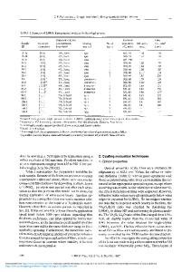
The fabrication process of an Al thin-film optical polarizer on LiNbO3 waveguides after CF4 plasma dry etching of a previously deposited SiO2 buffer layer was investigated. The problem in this process is a precipitation of compounds containing C, O, F, and Li on the etched LiNbO3 surface and a chemical deterioration of the Al caused by a reaction with these precipitates. Most notably, the growth of amorphous phase in addition to the crystalline Al metal grains and a partial oxidization of Al were found at the interface using transmission electron microscopy and x-ray photoelectron spectroscopy.
I. INTRODUCTION
The demand for LiNbO3 integrated optical waveguide devices has rapidly increased in order to realize the needs of high-speed communication systems. In this regard, processes unusual for LiNbO3 are sometimes attempted to improve the device performance.1,2 Plasma dry etching of the wafer surface is one of these uncommon processes, although it is a common process for semiconductor devices. Concerning dry etching of LiNbO3, we know of only a few reports on preparation of ridgelike waveguides on LiNbO3 by reactive ion etching (RIE) or by electron cyclotron resonance (ECR) plasma etching.3,4 Recently, we also have investigated the ECR etching of LiNbO3 surface with CF4 and CHF3 and found fluorination of the surface, a precipitation of LiF, and fluorocarbons.5,6 These fluoride precipitates were found to cause a weakening of bonding strength of the SiO2 buffer layer which was deposited on the etched LiNbO3 surface.7 We examine here another undesirable effect of the fluoride precipitates on CF4 plasma etched LiNbO3 surfaces in device fabrication processes. For instance, in x-cut LiNbO3 waveguide modulator devices, one can integrate an optical polarizer by depositing Al metal film on the Ti:LiNbO3 waveguides, which selectively propagates extraordinary light.8 On the other hand, a high-speed modulator needs a thick SiO2 buffer layer between waveguides and corresponding electrodes to adjust the speed of microwaves propagating in the
a)
e-mail: [email protected]
476
http://journals.cambridge.org
J. Mater. Res., Vol. 15, No. 2, Feb 2000 Downloaded: 01 Apr 2015
electrode. Because the SiO2 layer is annealed in O2 at higher temperatures after its deposition, the Al thin-film polarizer must be prepared after removing a part of the annealed SiO2 layer on the waveguide. As a method to make a window in the SiO2 film for direct Al deposition onto the LiNbO3
Data Loading...


