Chemical Vapor Deposition and Electrode Technologies for (Ba,Sr)TiO 3 Capacitor Used in Gigabit Dram
- PDF / 1,831,635 Bytes
- 8 Pages / 417.6 x 639 pts Page_size
- 29 Downloads / 282 Views
FOR (Ba,Sr)TiO 3 CAPACITOR USED IN GIGABIT DRAM K. Eguchi*, K. Hieda*, J. Nakahira**, M. Kiyotoshi*, M. Nakabayashi**, S. Yamazaki*, M. Izuha*, T. Aoyama*, K. Tsunoda***, J. Lin", K. Nakamura*, S. Niwa*, H. Tomita*, A. Shimada**, Y. Kohyama*, Y. Ishibashi*,Y. Fukuzumi*, T. Arikado*, K. Okumura* *Microelectronics Engineering Laboratory, Semiconductor Company, Toshiba Corporation, 8, Shinsugita-cho, Isogo-ku, Yokohama 235-8522, Japan, [email protected] "**Technology Development Division, Semiconductor Group, Fujitsu Limited, 1500, Mizono, Tado-Cho, Kuwana-Gun, Mie-ken 511-0192, Japan ***Fujitsu Laboratories Limited, 10-1, Wakamiya, Morinosato, Atsugi 243-0197 Japan
ABSTRACT We review our capacitor technology using (Ba,Sr)TiO 3 (BST) as a capacitor dielectric for dynamic random access memory (DRAM) application. Among a number of issues for BST capacitor process integration in DRAM cells, two important technologies are discussed. As an electrode technology, we propose All PErovskite Capacitor (APEC) technology, in which conducting perovskite oxide of SrRuO 3 (SRO) is used as capacitor electrodes. For chemical vapor deposition (CVD) of BST, we propose In-situ Multi-Step (IMS) process, which is a sequential repetition of low temperature deposition of ultra thin BST film and crystallization in the same chamber. By using APEC technology and IMS CVD process of BST, we can simultaneously achieve good electrical characteristics (low leakage current and high permittivity) and good step coverage. The combination of APEC technology and IMS CVD process of BST is a promising BST capacitor process technology for future DRAMs.
INTRODUCTION Although DRAM cell size has been rapidly decreasing each generation, the storage capacitance should remain constant in order to achieve stable DRAM operation. In order to keep storage capacitance constant for smaller cells, a significant effort has been devoted to thin IReliability
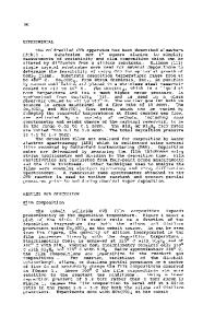
BST CVD
Si2
BSTal
Encapsulation
S•
Barri •
Backend damage process
SRO deposition ,02 and patterning
Barrier metal selection,W iT deposition, and patterning
iI
SiN
to sr t e
Barrier layer SiO2
W
S0
Fig. 1. BST capacitor structure and process issues. 3 Mat. Res. Soc. Symp. Proc. Vol. 596 © 2000 Materials Research Society
the standard SiN/Si0 2 capacitor dielectric and create larger capacitor area for same cell area by fabricating complicated three dimension cell structures such as trench cell, cylinder cell, multifin cell, etc. In the gigabit DRAM generation, however, it will be difficult to fabricate ever more complicated cell structures because the capacitor area will be very small and thinning of SiN/SiO2 dielectrics will be near its physical limitation. Another solution is to change the capacitor dielectric from SiN/SiO 2 to a new material which has a higher permittivity than SiN/Si0 2. (Ba,Sr)TiO 3 (BST) is a promising capacitor dielectrics for future DRAM capacitors in 0.10 - 0.13tm generations and a large effort has been devoted to develop BST capacitor for future DRAM cells[2-6]. F
Data Loading...