Comparison of High Field Characteristics of SiO 2 and AIN Gate Insulators in 6H SiC MOS Capacitors
- PDF / 392,035 Bytes
- 6 Pages / 414.72 x 648 pts Page_size
- 103 Downloads / 246 Views
ABSTRACT Using a fast ramp response technique, the high field characteristics, specifically the breakdown strength, of thermally grown silicon-dioxide (Si0 2) and MOCVD grown aluminum-nitride (AIN), on n-type 6H-SiC epilayers is obtained as a function of three different processing conditions for the insulator growth. Significant improvement in the breakdown strength of thermally grown Si0 2 after a 30 minute post annealing at 400'C in nitrogen ambient is reported. Further, the influence of temperature profile during the AIN growth on the breakdown strength is reported.
INTRODUCTION The reliability of MIS devices based on SiC is strongly dependent on the properties of the gate insulator, especially the high field characteristics such as breakdown strength. Due to large operating voltages, the electric field in gate insulators in MIS devices such as high power MOSFETs fabricated on SiC, could be significantly higher than that encountered in typical Si MOS devices. Hence, it is essential to optimize the gate insulator quality grown on SiC to minimize the leakage current under high fields. While the procedures for obtaining high quality Si0 2 on Si is well established, the properties of thermal oxide on SiC are far from ideal. Aluminum nitride has been suggested as a promising alternative for gate insulator on SiC [1-3]. The quality of the thermally grown SiO 2 and MOCVD grown AIN gate insulators have been characterized using classical capacitance (C)-voltage (V) characteristics as well as a high
field characterization technique known as the ramp response technique. The measurements were carried out on MIS capacitor structures fabricated on n-type 6H SiC wafers with - 5 gm thick epilayer of 10i5 - 1016 cm-3 doping concentration.
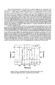
EXPERIMENT The fast-ramp response technique used for high field characterization involves the measurement of the current response in the accumulation and deep depletion regimes of a MIS capacitor structure while applying a rapid voltage ramp pulse [4]. While the accumulation mode measurements yield information about the conductivity and breakdown strength of the insulator layer, from the deep depletion measurements the maximum depth of the depletion layer (in the semiconductor) before avalanche breakdown, the maximum field in the semiconductor before avalanche generation is observed, etc. can be obtained. The experimental set-up used for the ramp response measurements is discussed in detail elsewhere [4]. For the accumulation measurements, a positive high voltage pulse is applied to the gate contact of the capacitor (for the n-type semiconductor), while the back ohmic contact is connected to ground via a 15k[ current viewing resistor (CVR). In this circuit configuration the applied voltage appears entirely across the insulator layer, and hence the characteristics of the insulator layer can be determined. Since the applied ramp voltage has a constant slope 345 Mat. Res. Soc. Symp. Proc. Vol. 512 ©1998 Materials Research Society
(dV/dt), for a fixed insulator capacitance (Ci.), the measured
Data Loading...