Control of the Si Vacancy Concentration and Arrangement in ReSi 1.75 by Al and P Additions
- PDF / 1,448,075 Bytes
- 6 Pages / 612 x 792 pts (letter) Page_size
- 98 Downloads / 234 Views
0980-II05-40
Control of the Si Vacancy Concentration and Arrangement in ReSi1.75 by Al and P Additions Shunta Harada, Katsushi Tanaka, Kyosuke Kishida, and Haruyuki Inui Department of Materials Science and Engineering, Kyoto university, Sakyo-ku, Kyoto, 6068501, Japan
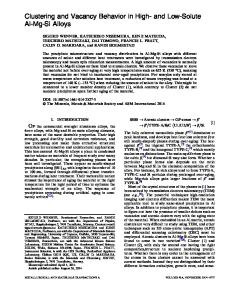
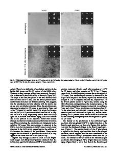
ABSTRACT The concentration and arrangement of Si vacancies in aluminum or phosphorus containing ReSi1.75 based silicides have been investigated. Both aluminum and phosphorus substitute for silicon. In addition to the (001)C11b twins usually observed in binary ReSi1.75, planar defects are heterogeneously formed in both of the ternary element . Using the high resolution electron microscopy (HREM) technique, the planar defects in aluminum and phosphorus _ containing ReSi1.75 are assigned crystallographic shear (CS) planes lying on ( 1 09) C11b and (107) C11b, respectively. The CS vector in both ternary alloys is [100]C11b. Since the concentration of vacancies in the ReSi1.75 structure is changed by the introduction of the crystallographic shear, the ternary alloys contain more or less amount of vacancies than the equivalent binary alloys. This implies that the concentration of Si vacancies changes in order to maintain the average number of valence electrons. Hence, ternary alloying can be used to control the concentration of Si vacancy in the ReSi1.75 based alloys. INTRODUCTION The semiconducting rhenium disilicide ReSi1.75 is known as a promising material for thermoelectric applications [1]. Various research results have been reported for the binary alloy of composition ReSi1.75, which can also be described as Re4Si7, regarding composition and crystal structure [2]. The crystal structure of rhenium disilicide has been reported as a tetragonal C11b (MoSi2-type, space group I4/mmm) structure and the stoichiometry was thought to be Re:Si=1:2 [3,4]. According to our recent analysis of high-resolution phase-contrast and Zcontrast images combined with first-principles calculation[5,6], however, the crystal structure is monoclinic with the space group of Cm due to an ordered arrangement of vacancies on Si sites in the underlying (parent) C11b structure. The crystal contains four differently oriented domains; two domains related to each other by the 90o-rotation about the c-axis of the underlying C11b lattice and twin domains for each of the two domains. The twin habit plane is (001) of the underlying C11b lattice and the thickness of twins ranges from 100~300 nm. Although the electrical transport properties of the disilicide have been reported by several researchers, they are controversial. Siegrist et al. [7] reported the value of Seebeck coefficients ranging from -90 to 130 µV/K at 310 K. On the other hand, Neshpor et al. [8,9] reported the value, which is in fair agreement with that reported by Siegrist et al. [7] but the sign is reversed. Our recent measurements on the electrical transport properties as well as thermal transport properties for the single crystals of ReSi1.75 indicated that the electrical resistivity along [001] shows a higher value than t
Data Loading...