Creep rupture induced silica-based nanofibers formed on fracture surfaces of Ti 3 SiC 2
- PDF / 636,402 Bytes
- 3 Pages / 612 x 792 pts (letter) Page_size
- 70 Downloads / 311 Views
T.J. Zhen and M.W. Barsoum Department of Materials Science and Engineering, Drexel University, Philadelphia, Pennsylvania 19104 (Received 21 January 2005; accepted 15 August 2005)
After creep failure at 1300 °C, silica-based nanofibers with diameters of ∼250 nm and lengths of up to a few tens of microns were observed on the fracture surfaces of Ti3SiC2. A possible mechanism for the formation of these fibers is proposed.
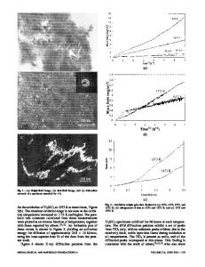
Ti3SiC2 is a representative compound of the Mn+1AXn (or MAX) phases, where M is an early transition metal, A is a group-A element, X is carbon and/or nitrogen, and n ⳱ 1–3. By now it is fairly well established that Ti3SiC2 possesses good electrical conductivity (4.3 × 10⁶ ⍀−1 m−1) and thermal conductivity (39.9 W/mK), is relatively soft (HV 4 GPa), machinable, damage tolerant, and resistant to thermal shock.1–6 Because of its good high-temperature mechanical properties and oxidation resistance,3,7,8 it is a promising candidate for high-temperature structural applications. For such applications, it is paramount to understand its creep response, which has been reported elsewhere.9,10 The purpose of this present article, however, is not to report on its creep behavior but to report on interesting features observed on fracture surfaces of samples that were crept at 1300 °C. Coarse-grained (grain size 30–50 m) Ti3SiC2 cylinders (9.8 mm in diameter and 31 mm long) were loaded under a compressive stress of 100 MPa at 1300 °C in air until rupture (for details see Ref. 8). The creep strain at rupture was ∼4%. The sample failed in a shear-like manner, with the fracture surface plane forming an angle of ∼45° to the loading axis. The fracture surface was observed with an FEI-XL30 field emission scanning electron microscope (SEM) equipped with an energydispersive spectrum (EDS) analyzer. Figure 1 shows an SEM micrograph of multiple nanofibers on the fracture surface. A higher magnification micrograph is shown in the inset. The nanofibers have a more or less circular cross-section, and appear as if they
a)
Address all correspondence to this author. e-mail: [email protected]; [email protected] DOI: 10.1557/JMR.2005.0381 J. Mater. Res., Vol. 20, No. 11, Nov 2005
http://journals.cambridge.org
Downloaded: 07 Apr 2015
were spun from a melt. Their diameter is ∼250 nm, and their lengths vary from a few to over 50 m. Figure 2 is an SEM micrograph of another set of nanofibers, where again the diameter is ∼250 nm. The lower inset magnifies the root of the nanofiber, which is reminiscent of a tree root. The upper inset shows a node in the nanofiber that became charged in the SEM as it was scanned with the electron beam at a slow scan speed, indicating that it most likely is an electric insulator. To determine the chemistries of various features shown in Figs. 1 and 2, individual nanofibers and faceted particles were retrieved from the fracture surfaces and affixed on a conductive carbon tape for EDS analysis. Figures 3(a) and 3(b) show the EDS spectra (with SEM micrographs as insets) of a single nanofiber (a) an
Data Loading...