Current limitation after pinch-off in AlGaN/GaN FETs
- PDF / 109,680 Bytes
- 4 Pages / 612 x 792 pts (letter) Page_size
- 74 Downloads / 205 Views
Internet Journal Nitride Semiconductor Research
Current limitation after pinch-off in AlGaN/GaN FETs R. Dietrich1, A. Wieszt1, A. Vescan1, H. Leier1, Joan M. Redwing2, Karim S. Boutros2, K. Kornitzer3, R. Freitag3, T. Ebner3 and K. Thonke3 1DaimlerChrylser AG,
Ulm, Germany,
2Epitronics/ATMI, 3Universität
Ulm, Abteilung Halbleiterphysik, Germany,
(Received Thursday, January 27, 2000; accepted Wednesday, March 22, 2000)
Piezoelectric AlGaN/GaN FETs on SiC with high carrier mobility have been fabricated yielding IDS=450 mA/mm and gm=200 mS/mm. In the on-state, under UV-illumination, the devices sustain a drain voltage of VDS=49 V, corresponding to a power dissipation of 26.5 W/mm. On turn-on of the device from the pinch-off state, a significant delay in the drain current build-up is observed. This effect depends on the pinch-off time and the pinch-off voltage and can be removed by either a brief UV-illumination or a VDS>25 V applied in the on-state. The drain current transients are characterized by a relaxation time τ, which is in the order of several hundred seconds. From the temperature dependence of τ, an activation energy of about 280 meV and a capture cross section of 4.4·10-18cm2 were determined. The devices show pronounced persistent photoconductivity (PPC) and the drain current ID is sensitive to illumination.
1
Introduction
Electronic devices based on GaN have attracted growing attention during the past years. This is mainly due to the promising material properties of GaN with respect to performance improvements for high-frequency power modules. To date, remarkable AlGaN/GaN FET-device results have been published with fmax≈140 GHz for small signals [1] and 6.9 W/mm output power density at 10 GHz [2]. To further increase the performance and provide reliable operation it is important to investigate possible limiting factors. In this report, we discuss a drain current delay effect and its removal by either a UV-illumination or by applying a high VDSto the device in the on-state . 2
Device fabrication
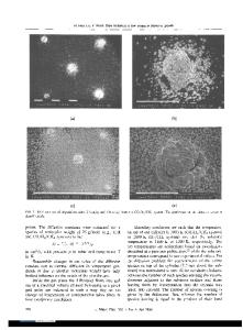
The epitaxial layer structure of the the FETs was grown in a vertical MOCVD reactor at 1100°C. A 100 nm AlN nucleation layer, a 3 µm GaN buffer and a 23 nm Al0.3GaN top layer were deposited on a (0001) n+-SiC substrate. No dopants were used. The undoped GaN buffer was deposited at a growth rate of 2 µm/h and a V/ III ratio of about 4000. These growth conditions resulted in a smooth surface morphology. Undoped layers grown under these conditions are typically highly resistive
(n25 V. Before measuring this trace, the device was pinched off at VGS0=-10 V for 5 min to get a pronounced current reduction (dotted line). The sudden removal of the current reduction at VDS>25 V can be explained by field enhanced carrier emission from traps. At VDS=25 V the electrical field between drain and gate is at least 20 MV/m. It is observed that the current reduction is influenced by the "history" of the gate voltage. Hence, the transients of the drain current ID at fixed drain and gate biases were studied for different gat
Data Loading...