Current-Voltage Characteristics of Ungated AlGaN/GaN Heterostructures
- PDF / 361,514 Bytes
- 6 Pages / 420.48 x 639 pts Page_size
- 25 Downloads / 300 Views
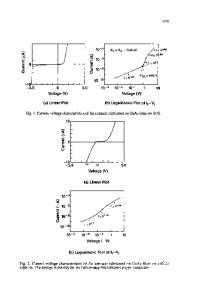
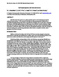
BSTRACT Results of a systematic study of the current vs. voltage characteristics of ungated AIGaN/ GaN heterostructures grown on sapphire substrates are presented. It is experimentally observed that the saturation current nearly doubles as the source-to-drain channel lengths decrease from 11.8 to 1.7ltm. The average electric field at which current saturation occurs is 10 to 30kV/cm, i.e. much less than the electron velocity saturation field. The experimental data is interpreted in the framework of a new model that takes into account the non-uniformity of the electron density in the channel, electron velocity saturation, and thermal effects. The temperature dependent electron transport characteristics of the model are based on Monte Carlo simulations of electron transport in GaN. It is shown that appreciable contact resistance, which leads to partial channel depletion near the source, and significant self-heating of the devices under high drain-to-source bias are the main reasons for the observed current saturation. The effective ambient temperature in the channel of the devices is calculated from a two-dimensional thermal model of heat dissipation through the sapphire substrate. Equilibrium channel carrier concentrations and low-field mobilities are determined from Hall effect data. The ungated structures are demonstrated to provide much useful materials and process characterization data for the development of AIGaN/GaN heterostructure field effect transistors.
INTRODUCTION AIGaN/GaN heterostructures have excellent potential for the realization of high-power, high-frequency heterostructure field effect transistors (HFETs) [1,2,31. The GaN channel material is characterized by favorable electron transport parameters, such as high mobility and high peak velocity. In addition, polarization charges at the hetero-interface can neutralize a large electron charge density, thus allowing for high channel carrier concentrations. However, most epitaxial 111-nitride structures are currently grown on sapphire substrates. Sapphire has a relatively low thermal conductivity and, consequently, the performance of AlGaN/GaN HFETs that are heatsunk through the sapphire substrate has been shown to be limited by deleterious thermal effects at high voltages and currents [4]. Furthermore, the fabrication technology for these devices is still relatively immature. Hence, contact resistances are often large and can seriously impair device performance [4].
489 Mat. Res. Soc. Symp. Proc. Vol. 572 © 1999 Materials Research Society
Ungated HFET structures are of interest as simple characterization structures used in, e.g., transmission line method (TLM) determinations of the equilibrium sheet resistivity and contact resistance, and as saturated resistors in some circuit application. Here, we present a systematic theoretical and experimental examination of ungated A1GaN/GaN heterostructures grown on sapphire substrates. 12
DEVICE STRUCTURE
"4
10 o
The III-nitrides used in this study were grown by MOCVD on sapphire substrates. The material st
Data Loading...