Defect investigation of GaN thin films etched by photo-electrochemical and hot wet etching by atomic force and transmiss
- PDF / 2,014,246 Bytes
- 6 Pages / 612 x 792 pts (letter) Page_size
- 16 Downloads / 273 Views
Defect investigation of GaN thin films etched by photo-electrochemical and hot wet etching by atomic force and transmission electron microscopy P. Visconti 1,2, K. M. Jones, M. A. Reshchikov, R. Cingolani 2, and H. Morkoç Virginia Commonwealth University, Dept. of Electrical Engineering, Richmond, VA, 23284 1 Also with: Istituto per lo Studio di Nuovi Materiali per l’Elettronica, CNR, 73100, Lecce, ITALY 2 Also with: INFM and Dept. of Innovation Engineering, Univ. of Lecce, 73100, Lecce, ITALY
R. J. Molnar Massachusetts Institute of Technology, Lincoln Laboratory, Lexington, MA 02420-9108
D. J. Smith Dept. of Physics and Astronomy and Center for Solid State Science Arizona State University, Tempe, AZ 85287
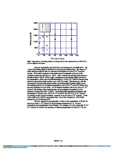
ABSTRACT The availability of reliable and quick methods to investigate defects in GaN films is of great interest. Photo-electrochemical (PEC), and hot wet etching using both H3PO4 acid and molten KOH have been used to study structural defects in GaN layers grown by hydride vapor phase epitaxy and molecular beam epitaxy. The purpose of this work is to determine whether, and under what conditions, these different methods of investigation are consistent and to get to a more accurate estimation of the defect density. As-grown and etched surfaces were investigated by atomic force microscopy (AFM), and plan-view and cross-sectional transmission electron microscopy (TEM). Free-standing whisker-like features and hexagonal etch pits were formed on the etched sample surfaces by PEC and wet etching, respectively. Using plan-view AFM, we found the density of whiskers (8x10⁸-1x109 cm-2) to be similar to the etch pit densities when etched in both H3PO4 and molten KOH under precise etching conditions. During the wet etching process, a careful balance must be struck to ensure that every defect is delineated, but not overetched to cause merging which would lead to an underestimation of the defect density. Additionally, TEM observations confirmed the dislocation densities obtained by etching, which increased our confidence in the consistency of the methods used. INTRODUCTION Achievement of GaN-based photonic and electronic devices with high performance and longevity requires epitaxial films with low defect density [1,2]. The most commonly used substrates such as sapphire and silicon carbide poorly match with GaN material in both lattice parameter and thermal expansion coefficient resulting in a high density (108-1010 cm-2) of threading dislocations [3,4,5]. It has been demonstrated that these defects affect both electrical and optical properties of the material [6,7]. Mostly, the characterization of the dislocations in nitride films is carried out using plan-view and cross sectional transmission electron microscopy (TEM) analysis, a process that however requires extensive sample preparation. Therefore the availability of reliable and quick methods in order to investigate the structural defects and to get to a estimation of their density is of great importance. Wet chemical etching is a convenient technique for the analysis of st
Data Loading...