Determination of the Strain Status of GaAs/AlAs Quantum Wires and Quantum Dots
- PDF / 378,235 Bytes
- 6 Pages / 414.72 x 648 pts Page_size
- 80 Downloads / 390 Views
2'- 2. 0
ý-SL-"' (004)
IJ
- (a)
-2-
-2
11
.1
Is
(b) _
Ile_
CuKax1 -1
_
__________
0
q, (10A-'/-1)
1
-1
_
__
0 A-') 1 q, (10-3
2
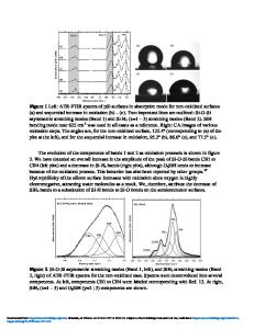
Fig.l: Reciprocal space maps of the reference sample (a) and the wire array (b) around the GaAs (004) reflection. an etching depth of approximately 760 nm. This implies, that the 1 gm GaAs buffer was partly etched, whereas the buried short-period SL and the GaAs substrate were not structured. A Philips MRD diffractometer, with a four crystal Ge (220) monochromator and a channel cut two crystal Ge (220) analyzer, was used with an angular resolution of 12 arc seconds. The independent variation of the two diffraction angles co (between incident x-rays and sample surface) and 20 (between incident and scattered x-rays) provides the possibility of reciprocal space mapping, i.e., the acquisition of twodimensional projections in the three-dimensional reciprocal space. RESULTS AND DISCUSSION Fig.1 (a) shows a reciprocal space map around the (004) reciprocal lattice point (RELP) of an unstructured (as grown) GaAs/AlAs-reference sample. "S"denotes the GaAs-substrate peak, SLo and SLi the zero and first order MQW-peak, respectively. "A" is a symbol for the analyzer streaks, these TAD artefacts have count rates of typically less than 3 counts per second (cps). RELPs with high intensity, in the present example the substrate reflection S and the SLo peak, are elongated along the Ewald sphere intersecting the growth direction with Bragg angle OB. Thickness fringes in-between the MQW-peaks SLo and SL1 indicate the good crystalline quality of the system. Their spacing (see Fig.1 a) corresponds to the total thickness of the superlattice of approximately 640 nm. From the spacing of the intensity extrema of the zeroth and first order MQW satellites (SLo and SL1) the MQW period was determined to be 21.3 nm. In Fig.1 (b) the diffraction pattern of the periodic wire array is shown. Wire satellites accompanying the SLo peak and the first order MQW-peak SL1 are observed. The regions around SLo and SL1 have been measured separately in order to save integration time. The wire period determined from the spacing of the satellites along qx-direction is 303 nm. The satellites beside the GaAs substrate and buffer peak indicate a corrugation (partial etching) of the GaAs buffer. The half width of these fringes is much larger than that of the actual GaAs/AlAs dot fringes. Consequently, the etching depth of the buffer is smaller, between 100 and 200 nm.
976
In Fig.2 maps for the periodic dot array are shown. The sample was oriented with the [110] direction perpendicular to the diffraction plane (qx-direction coincides with [1 -10], (a)) and with [100] perpendicular to the diffraction plane (qx-direction coincides with [010], (b)). Clearly dot satellites are observable both around the SLo satellite RELP and the GaAs buffer peak (Di denotes their respective order). The satellite spacing decreases by a factor of 1/[2, if the diffraction plane is rotated by 45 degrees out of one principal direction of t
Data Loading...