Deviation of the mechanical response of wall-patterned GaAs surface: a central-plastic-zone criterion
- PDF / 673,597 Bytes
- 6 Pages / 612 x 792 pts (letter) Page_size
- 54 Downloads / 249 Views
0904-BB05-09.1
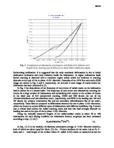
Deviation of the mechanical response of wall-patterned GaAs surface: a central-plastic-zone criterion E. Le Bourhisa, G. Patriarcheb a Université de Poitiers, Laboratoire de Métallurgie Physique, UMR 6630 CNRS, SP2MITéléport 2-Bd Marie et Pierre Curie, B.P. 30179, 86962 Futuroscope-Chasseneuil Cedex, France b Laboratoire de Photonique et de Nanostructures, UPR 20 CNRS, Route de Nozay, 91460 Marcoussis, France ABSTRACT Wall-patterned GaAs surfaces have been elaborated by photolithography and dry etching. Different surfaces were produced in order to change the aspect ratio of the walls formed at the substrate surface. The mechanical behaviour of individual walls was investigated by nanoindentation and the responses were compared to that of a standard bulk reference (flat surface). Deviation from the bulk response is detected in a load range of 0.1-25 mN depending on the aspect ratio of the walls. A central-plastic-zone criterion is proposed in view of TEM images of indented walls and allows predicting the response deviation of a given wall knowing its width. The application of substrate patterning for optoelectronic devices is proposed in the perspective of eliminating residual dislocations appearing in mismatched structures. INTRODUCTION Plasticity of III-V semiconductors has received much attention during the past two decades because of the needs from the optoelectronic industry. In fact, developments of heterostructures for such applications have been limited as plastic relaxation deteriously affects the performance of the devices. As a matter of fact, a better understanding of III-V semiconductors plasticity at temperatures used for devices elaboration (RT-500°C) is required and will be of great help to improve substrate ‘compliance’ and heterostructure quality [1]. As the sizes of the structures are decreasing progressively, plasticity of finite volumes is to be understood. In this field, the indentation technique has proved to be a powerful tool to test small volume even at temperature below the brittle-ductile transition (for a review refer to Ref. [2]). Furthermore, contact mechanics has been developed for semi-infinite half space [3]. This assumption is not fulfilled when the size of the plastic zone becomes of the order of one of the dimensions of the object [48]. Thereafter, thin structures are expected to show a mechanical behaviour quite different from that of a bulk. It has been known for long that yield strength of metallic alloys can be improved with the refinement of the grain size [9,10]. However, length scale induced changes in the response of a single object has been poorly addressed. Only recently, nanoindentation studies of single polycrystalline Al lines deposited onto a Si substrate and focussed-ion beam (FIB) milled Ni cylinders were reported in the µm- length scale [4,5,8]. In the field of semiconductors recent studies showed that indeed, when the contact depth to thickness ratio hc / e approaches 3 %, a free standing film cannot be considered as a semi-infinite half space any
Data Loading...