Drastic Change in the GaN Film Quality by In-Situ Controlling Surface Reconstructions in GSMBE
- PDF / 1,647,654 Bytes
- 4 Pages / 414.72 x 648 pts Page_size
- 76 Downloads / 304 Views
* e-mail-address: [email protected] ABSTRACT
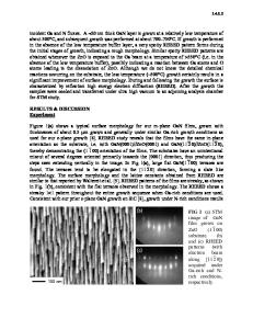
GaN growth was performed on 6H-SiC (0001) substrates by gas-source molecular beam epitaxy (GSMBE), using ammonia (NH 3) as a nitrogen source. Two kinds of reflection high-energy electron diffraction (RHEED) patterns, named (lxl) and (2x2), were observed during the GaN growth depending on the growth conditions. By careful RHEED study, it was verified that the (lxl) pattern was corresponded to a H2-related nitrogen-rich surface, while (2x2) pattern was resulted from a Ga-rich surface. By x-ray diffraction (XRD), photoluminescence (PL) and atomic force microscopy (AFM) characterizations, it was found that the GaN quality changed drastically grown under different RHEED patterns. GaN film grown under the (lxl) RHEED pattern showed much better qualit•es than that grown under the (2x2) one.
INTRODUCTION Wide band-gap GaN and related I1-V nitride materials have shown a strong potential for use in optical devices, especially blue and ultraviolet light emitting diodes (LEDs) and laser diodes (LDs)[1]. InGaN multi-quantum-well laser diodes under room-temperature continuous wave operation was successfully fabricated, and the threshold current and voltage of the LDs were 160 mA and 6.7 V, respectively[2]. Employment of 6H-SiC substrates for the growth of GaN provides a number of advantages such as small lattice mismatch (about 3%), compared to sapphire's (A120 3, about 13.8%), as well as potential for the formation of Fabry-Perot cavities by cleaving. Molecular Beam Epitaxy (MBE) growth technique has been shown to be one of the most successful tool for growing such kind of materials. Lin et al[3] reported that AIN coated (0001) 6H-SiC substrates are excellent candidates for GaN growth. Their results showed that the quality of GaN film was better on (0001) 6H-SiC substrates than that grown on A120 3 (0001) ones by electron mobility and XRD measurements. Korakakis et al. [4] also reported the direct growth of GaN on (0001) 6H-SiC substrates without AIN or GaN buffer layers. In these studies, ECR plasma nitrogen source was employed and a (2x2) RHEED pattern of GaN was observed. However, by using ECR or rf source, the growth rate of GaN is slow in general. By comparison, it isrelatively easy to dissociate NH 3,where the molecular break-up process can be achieved easily on a heated GaN surface, which is named on surface cracking (OSC)[5]. Yang et al[6] reported the GaN growth on A120 3 (0001) substrates using NH 3 and they demonstrated the growth rate as high as 1000 nnmlr. Using NH 3 as the predominant nitrogen source with additional ECR nitrogen plasma, high quality p-type Mg-doped GaN film were achieved without the need for post-growth annealing. Although them are many merits by using (0001) 6H-SiC substrates and NH 3, there are little reports concerning the growth and characterizations of GaN films grown on the substrate using NH 3 as a nitrogen source. In this paper, we report the GaN growth on (0001) 6H-SiC substrates with a thin AN buffer 223 Mat. Res. Soc. Symp. Proc. Vol. 4
Data Loading...