Evaluation of Sputtering Deposited 2-Dimensional MoS 2 Film by Raman Spectroscopy
- PDF / 406,843 Bytes
- 6 Pages / 432 x 648 pts Page_size
- 3 Downloads / 316 Views
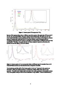
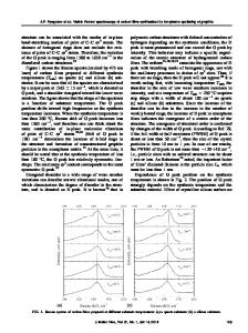
Evaluation of Sputtering Deposited 2-Dimensional MoS2 Film by Raman Spectroscopy S. Ishihara1, K. Suda1, Y. Hibino1, N. Sawamoto1, T. Ohashi2, S. Yamaguchi2, K. Matsuura2, H. Machida3, M. Ishikawa3, H. Sudoh3, H. Wakabayashi2, and A. Ogura1 1 School of Science and Technology, Meiji University, 1-1-1 Higashimita, Tama-ku, Kawasaki, Kanagawa 214-8571, Japan. 2 Interdisciplinary Graduate School of Science and Engineering, Tokyo Institute of Technology, 4259 Nagatsuta-cho, Midori-ku, Yokohama, Kanagawa 226-8502, Japan. 3 Gas-phase Growth Ltd, #301 Nokodai-Tamakoganei Venture Port, 2-24-16 Naka, Koganei, Tokyo 184-0012, Japan. ABSTRACT Molybdenum disulfide (MoS2), one of the transition-metal dichalcogenides, is a 2-dimensional semiconducting material that has a layered structure. Owing to excellent optical and electronic properties, the ultra-thin MoS2 film is expected to be used for various devices, such as transistors and flexible displays. In this study, we investigated the physical and chemical properties of sputtered-MoS2 film in the sub-10-nm region by Raman spectroscopy and X-ray photoelectron spectroscopy (XPS). As the results of Raman spectroscopy investigations, we observed two Raman modes, E12g and A1g, in the 2-dimensional MoS2 films. As the thickness of the MoS2 film decreased, the peak frequency difference between E12g and A1g modes increased. From the XPS investigations, we confirmed sulfur reductions from the 2-dimensional MoS2 films. Therefore, we considered that the sulfur vacancies in the MoS2 film affected the Raman peak positions. Moreover, we performed the additional sulfurization of sputtered-MoS2 films. From the XPS and Raman investigations, the quality of the sputtered-MoS2 films was improved by the additional sulfurization. INTRODUCTION Molybdenum disulfide (MoS 2), one of the transition-metal dichalcogenides, is a 2-dimensional semiconducting material that has a layered structure. It is known that MoS2 shows different physical properties depending on the number of layers. Single-layer MoS2 has a direct band gap (Eg=1.8 eV), while bulk MoS2 has an indirect band gap (Eg=1.2 eV) [1-7]. In addition, single-layer MoS2 transistors show excellent properties. For example, it is reported that the field-effect mobility in single-layer MoS2 transistor was as high as 217 cm2V-1s-1 [8]. Owing to these optical and electronic properties, the ultra-thin MoS2 film is expected to be used for various devices, such as transistors and flexible displays. We fabricated 2-dimensional MoS2 films by sputtering deposition. In general, the sputtering deposition has a superior mass productivity and the film thickness can be controlled accurately only by the deposition duration. Although sputtered-MoS2 film has been used as solid lubricant [9-17], details of the sputtered-MoS2 thin film for device applications have not been revealed sufficiently yet. In our previous work, we achieved to form a five-layer MoS2 on SiO2 substrate by sputtering deposition, and confirmed that its carrier density can be dramatically decreased com
Data Loading...