Evolution of Coherent InAs Quantum Dots Above the Coherent Critical Thickness Window by Metalorganic Chemical Vapor Depo
- PDF / 958,116 Bytes
- 5 Pages / 612 x 792 pts (letter) Page_size
- 97 Downloads / 333 Views
Evolution of Coherent InAs Quantum Dots Above the Coherent Critical Thickness Window by Metalorganic Chemical Vapor Deposition T. S. Yeoh,1 C. P. Liu,2 Y. W. Kim,3 and J. J. Coleman1 1
Semiconductor Laser Laboratory, University of Illinois at Urbana-Champaign 208 N. Wright Street, Urbana, IL 61801, U.S.A. 2 National Cheng Kung University Tainan, TAIWAN. 3 Materials Research Laboratory, University of Illinois at Urbana-Champaign 104 S. Goodwin Ave. Urbana, IL 61801, Urbana, IL.
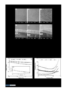
ABSTRACT InAs quantum dots were grown on GaAs substrates at various coverages and capped after varying the time of growth interruption. The evolution of this system was examined by correlating photoluminescence and transmission electron microscopy measurements. Results show for the first time the growth interruption to be a critical factor in generating defect-free quantum dot ensembles at coverages well above established metalorganic chemical vapor deposition coverage window for defect-free, Stranski-Krastanow self-organized growth. In addition, our results also support the absence of a stable, dislocation free 3D state and that the chemical potential eventually drives the system towards dislocated quantum dot clusters. INTRODUCTION The evolution of Stranski Krastanow (S-K) grown InAs quantum dots (QDs) on GaAs has attracted much attention in recent times due to its ability to create high quality quantum ensembles for use in quantum dot devices.1-3 Understanding the evolution of such materials is now of great importance as recent evidence has shown that once the critical layer thickness (CLT) of the strained film is reached, the surface chemical potential drives the system from a flat film towards coherent islands and ultimately towards dislocated island clusters.4 In the present study, the evolution of this InAs/GaAs system was examined by varying the initial coverage above the CLT and by varying the subsequent growth interruption times. EXPERIMENTAL DETAILS The samples were grown in a Thomas Swan atmospheric pressure metalorganic chemical vapor deposition reactor with a vertical rotating succeptor using TMIn, TMGa and AsH3 sources on (001) (±0.5°) oriented semi insulating GaAs wafers. The substrates were heated to 800 °C for 10 minutes to allow for native oxide desorption before being cooled to 625 °C where a GaAs buffer layer of 0.1 µm was grown. They were then cooled to 450 °C before various coverages of InAs were deposited at a rate of ~0.5 monolayers (ML) per second, after which the samples were subjected to a growth interruption of various times under H2 ambient before being capped with 0.1 µm of GaAs. The QD density was determined using atomic force microscopy (AFM), and the densities of dislocated quantum dots were determined using strain-field transmission electron microscopy (TEM). The total deposited InAs thickness was determined using Rutherford O8.7.1
Backscattering (RBS). The photoluminescence (PL) measurements were performed using a liquid nitrogen-cooled germanium detector and excited using a 514 nm argon laser. DISCUSSIO
Data Loading...