Fabrication and Characterization of InGaN Nano-scale Dots for Blue and Green LED Applications
- PDF / 89,304 Bytes
- 5 Pages / 612 x 792 pts (letter) Page_size
- 13 Downloads / 281 Views
F99W11.74
(a)
(b)
(c)
(d)
(e)
(f)
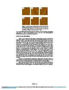
Figure 1, AFM images of InGaN films with the growth time (nominal thickness) of (a) 0 sec (0 nm), (b) 3 sec (0.15 nm), (c) 12 sec (0.57 nm), (d) 24 sec (1.15 nm), (e) 48 sec (2.3 nm), and (f) 3600 sec (400 nm). Scan areas are 4 × 4 um2. 5 nm, InGaN SQW applying different growth conditions, and a 30 nm-thick GaN capping layer grown at 1100 oC. The precursors of Ga, In, Si, and N are trimethylgallium, trimethylindium, silane, and ammomia, respectively. RESULTS AND DISCUSSION Figure 1 (a) – (f) show the AFM images of morphological evolution of InGaN thin films grown at 800 oC, which are dependent on the growth times (thickness) from 0 sec to 3600 sec. Typical surface shape for n-type GaN, including steps, terraces, and surface dislocations, is shown in Fig. 1 (a). The small surface dislocations observed are 37 nm in size and 0.5 - 1 nm in height. The density of surface dislocations is 4 – 5 X 109 cm-2, which shows good agreement with the dislocation density measured by the TEM. Many of them are lie along the step boundaries. As the nominal thickness of InGaN films increase from 0.15 to 1.15 nm, one can clearly see that 2 D (corresponding to wetting layer) to 3 D (self-assembled QD) transition, which is direct evidence of StranskiKrastanov (S-K) growth mode of InGaN epilayer. For the case of QDs shown in the InGaN film with the thickness of 0.57 nm and 1.15 nm, the average lateral size and height of dots are 73 nm, 2 nm, and 78 nm, 3.7 nm, respectively. Especially, the density (4 X 109 cm-2) of QDs shown in Fig. 1 (c) is nearly same with that of surface dislocations of low-temperature grown GaN. However, we have confirmed they have no correlation each other (see Fig. 2 (a)). If the thickness more increases, the size of the InGaN nanoscale dots is increased and the InGaN film shows polycrystalline growth mode or cluster formation. From the x-ray photoelectron spectroscopy measurement (not shown here), we observed that In 3d peaks intense with increasing the thickness of InGaN thin films. This result shows that In surface segregation is occurred during the InGaN growth[6]. Figure 2 (a) and (b) show a plan-view HRTEM and a cross sectional HRTEM (XHRTEM) image of the sample in Fig. 1 (c). The most important feature in (a) is that the nano-scale dots are formed irrespective of dislocation indicated by an arrow. Especially,
F99W11.74
(1-102) 35o
InGaN
QD
GaN
(a)
(b)
10 nm
Figure 2, (a) Plan-view HRTEM weak beam image and (b) X-HRTEM image of 0.57 nm-thick InGaN thin film. Arrow shown in (a) indicates dislocations.
Normalized PL Intensity (arb. units)
knowledge of the shape of self-organized InGaN/GaN QDs is needed to constrain theoretical calculations of the process formation as well as electronic structure. For the heteroepitaxial growth suffering large lattice mismatch like InAs/GaAs and Ge/Si, several quantum dot shapes, namely conical[7], square-base pyramid[8], prism-like cluster[9], triangular shape [10] etc., have been reported. Figure (b) shows that the InGaN nano
Data Loading...


