Femtosecond Laser-induced Crystallization in As-deposited Ge 1 Sb 2 Te 4 Films
- PDF / 396,074 Bytes
- 6 Pages / 612 x 792 pts (letter) Page_size
- 36 Downloads / 325 Views
HH5.7.1
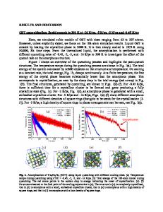
Femtosecond Laser-induced Crystallization in As-deposited Ge1Sb2Te4 Films Qin F. Wang1, 2, Lu P. Shi2, Su M. Huang2, Xiang S. Miao2, Kai P. Wong2 and Tow C. Chong1, 2 1 Department of Electrical and Computer Engineering, National University of Singapore, 4 Engineering Drive 3, Singapore 117576 2 Data Storage Institute, DSI Building, 5 Engineering Drive 1, Singapore 117608 ABSTRACT Time resolved imaging has been used to investigate the whole process of the crystallization induced by intense 130 femtosecond laser pulses in as-deposited Ge1Sb2Te4 films. With an average fluence of 24mJ/cm2, a transient non-equilibrium state of the excited material is formed within 1 picosecond. The results are consistent with an electronically induced non-thermal phase transition. INTRODUCTION Femtosecond (10-15s) laser can generate the most extreme non-equilibrium conditions and give rise to novel and unusual phase transitions. It also can afford high temporal resolution for observation and study of fundamental processes in femtosecond time scale. Thus the interaction of femtosecond laser with materials has been extensively studied during the past two decades. Femtosecond pulse is very promising for optical data storage due to high data transfer rate, efficient delivery of optical power, enhancement of the cooling rate and extreme suppression of the thermal diffusion effects. Ohta et al. 1 first demonstrated that single 120fs laser pulse could induce an amorphous mark at crystalline background accurately in the laser spot without the crystalline edge in GeTe-Sb2Te3-Sb sandwich structure. Our previous investigations2 further exhibited that amorphization or crystallization induced by femtosecond laser could be achieved by proper controlling the thickness of Ge1Sb2Te4 films. In this study, time-resolved microscope was used to measure transient reflective intensity in order to reveal the entire process and gain insight into the mechanism of crystallization induced by femtosecond pulse in as-deposited Ge1Sb2Te4 films. EXPERIMENTAL CONDITIONS Our in house developed Phase Change Optical Disk Design software3 was used to design the multilayer structures in order to obtain good contrast between amorphous and crystalline states of 100nm Ge1Sb2Te4 films at 800nm. The sample structure used in this experiment was: 0.6mm polycarbonate substrate/ (ZnS)80(SiO2)20 120nm/Ge1Sb2Te4 100nm/ (ZnS)80(SiO2)20 92nm/ air The sample was fabricated by a Balzers Cube sputtering system, which is guided by windows-based software. The system has four independent process chambers and three sputtering power sources (two DC and one RF). The Ge1Sb2Te4 was sputtered using the DC magnetron sputtering method. The (ZnS)80(SiO2)20 dielectric layers were sputtered by the RF
HH5.7.2
sputtering method. The distance between the target and substrate was 4cm, the chamber background pressure was below 1.2x10⁻⁷ mbar, and the sputtering pressure of Ar gas was approximately 4.5-5.5x10⁻³ mbar. The evolution of the transient reflective intensity of the irradiated surface was m
Data Loading...