Formation of highly oriented diamond film on carburized (100) Si substrate
- PDF / 1,352,586 Bytes
- 7 Pages / 576 x 792 pts Page_size
- 70 Downloads / 323 Views
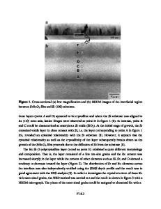
Highly oriented diamond film was grown on a (100) Si substrate by a bias-enhanced microwave-plasma chemical vapor deposition. The Si surface was carburized at a faster rate by bias treatment than by carburization alone, but the initial carburization stage was indispensable. During the bias treatment, the flat surface was changed to a textured structure on the nanometer scale. The formation of this structure was required for the synthesis of a highly oriented diamond film. Diamond microcrystals formed subsequently were irregular and of a few to a few tens nanometers in size. They then grew to oriented film in the following growth process.
I. INTRODUCTION The formation of large-area single-crystalline films is a goal of CVD diamond research because of their great potential in microelectronic device technology.1'2 Although mirror-polished silicon (Si) is one of the most practical substrates for diamond deposition, the population density of diamond particles formed on this substrate is normally as low as 104—105 cm" 2 . Thus, a variety of substrates and pretreatment methods have been tested. Recently, Yugo et al? found that a negative bias treatment was very effective for enhancing the nucleation of diamond. Employing this biasenhanced microwave-plasma chemical vapor deposition (bias-enhanced MPCVD) technique, several groups succeeded in controlling the orientation of diamond particles on mirror-finished SiC or Si substrates. Stoner et al.4'5 first obtained a textured diamond film on a /3-SiC film that was grown epitaxially by a thermal CVD method6'7 on a (100) Si substrate, prior to the bias-enhanced MPCVD. Kohl et al} also synthesized a textured diamond film in the same way. In their experiments, the surface of the SiC film was carefully modified by sophisticated pretreatments. On the other hand, Wolter and co-workers9 developed a three-step deposition process consisting of (i) in situ carburization of a mirror-finished Si surface, (ii) precise controlled nucleation under negative biasing, and (iii) growth without biasing. By this technique, a highly oriented boron-doped diamond film was grown on a (100) Si substrate.10 The hole mobility of the film at room temperature was 165 cm 2 /(V • s), which was approximately five times greater than that of polycrystalline films. This in situ process seems to be
a)
Author to whom correspondence should be addressed.
158
J. Mater. Res., Vol. 10, No. 1, Jan 1995
http://journals.cambridge.org
Downloaded: 18 Mar 2015
very promising for the production of large-area singlecrystalline diamond films, although the relationship between orientation of diamond and process conditions, particularly in the bias-enhanced nucleation step, is not fully elucidated to date. Jiang et al.11'12 formed a highly oriented diamond film on a mirror-polished (100) Si wafer. The substrate was also treated in situ by applying a negative bias in a microwave plasma. These results reveal that controlled nucleation under negative biasing is a key technique for the highly oriented diamond, but details of b
Data Loading...