Graphene Channels Interfaced with Quantum Dots in Field Effect Transistors: Electrical and Photo-Induced Effects
- PDF / 1,046,713 Bytes
- 7 Pages / 432 x 648 pts Page_size
- 2 Downloads / 288 Views
Graphene Channels Interfaced with Quantum Dots in Field Effect Transistors: Electrical and Photo-Induced Effects
Xin Miao1, Samarth Trivedi2, and Haim Grebel1 Electronic Imaging Center and ECE Dept., New Jersey Institute of technology (NJIT), Newark, NJ 07102, U.S.A 2 Department of Chemistry, New Jersey Institute of technology (NJIT), Newark, NJ 07102, U.S.A [email protected]
1
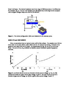
ABSTRACT Graphene-based field effect transistors (GFETs) were assessed when interfaced with well separated and precisely placed core/shell CdSe/ZnS semiconductor quantum dot (QD) arrays. The QDs were imbedded in a hexagonal hole-array, which was formed in a layer of anodized aluminum oxide on Si/SiO2 substrates. Graphene (single, or two layers), grown by chemical vapor deposition (CVD) on Cu foils, was transferred and placed on top of the QDs imbedded films and served as the transistor channel. Electrical characteristics under white-light illumination at various biasing conditions revealed that the photo current was decreasing upon increasing biasing. The device's photoluminescence (PL) as a function of both the drain-source and gate-source potentials also reduced as a function of the potential biases. We observed two maxima in the PL data while tilting the sample with respect to the incident laser beam. We attributed it to the optimal coupling between the incident and the emission wavelengths to resonating surface modes. INTRODUCTION Graphene - a two-dimensional atomic layer of graphite - has outstanding physical properties: high conductivity, chemical inertness, mechanical robustness and unusual electronic dispersion relations [1]. The electrical properties of free-standing graphene layer(s) have been studied in the past when deposited over nano-pore arrays, which were formed in anodized aluminum oxide (AAO) [2-3]. Raman spectra of the graphene lines were accentuated by the hole-array, as well. The periodic array of nano-pores has led to the realization of the first visible surface plasmon laser [4-6]; there, one takes advantage of simultaneous resonating plasmon/polariton modes in both the pump and the emission frequencies. Here, we took advantage of surface modes, which were propagating along the graphene channels. We analyzed the effect of electrical bias on the PL of well-separated and pore imbedded core/shell CdSe/ZnS semiconductor QDs when interfaced with one or two-layer graphene channels. The interplay between the electrical and optical bias of the channel may lead to new opto-electronic elements. EXPERIMENT Depicted in Figure 1a, we started with Si/SiO2 substrates. The p-type Si wafer was serving as the back-gate electrode. The silicon substrates were deposited with 150 nm of SiO2 using plasma assisted CVD. A 250 nm thick layer of aluminum was evaporated on top of the
1597 Downloaded from https:/www.cambridge.org/core. IP address: 80.82.77.83, on 05 Jul 2017 at 17:29:18, subject to the Cambridge Core terms of use, available at https:/www.cambridge.org/core/terms. https://doi.org/10.1557/adv.2016.106
SiO2 substrates. The aluminu
Data Loading...