Growth and Characterization of Semicontinuous Metal Films by Pulsed Laser Ablation
- PDF / 88,645 Bytes
- 6 Pages / 612 x 792 pts (letter) Page_size
- 59 Downloads / 330 Views
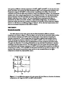
Growth and Characterization of Semicontinuous Metal Films by Pulsed Laser Ablation S.K. So, H.H. Fong, and N.H. Cheung Department of Physics, Hong Kong Baptist University Kowloon Tong, Hong Kong China ABSTRACT Semicontinuous metals films of copper and gold were grown on different substrates by pulsed laser ablation. The resistance and transmittance of these growing metal films were monitored in situ vs film thickness. Despite diverse experimental variations, it was found that both resistance and transmittance exhibited similar behaviors. Around percolation, the resistance exhibited a sharp drop whereas the transmittance exhibited a dip. In general, the onset of percolation depended on laser fluence and substrates. Under favorable conditions, metal films as thin as 1.5 nm would percolate. INTRODUCTION Semicontinuous metal films are subjects of uninterrupted interest for nearly a century [1]. From a modern perspective, they can be viewed as a form of semi-connected metal nanoclusters on an insulated substrate. The nominal thickness (τ ) of a semicontinuous film is of the order of 1-10 nm. In general, τ is highly dependent on the growth conditions and on the metal-substrate interaction. Within a semicontinuous metal film, there exist many paths that connect one end of the film to the other, but the average path length is much larger than the lateral dimension of the film. Hence the resistance of a semicontinuous film is intermediate between a bulk film and the insulating substrate. Typical resistance values vary from mega to tens of ohms. Renewed interests in semicontinuous films arise recently due to observations of their very intriguing optical properties. Examples were the observation of unusual optical behaviors near percolation, such as enhanced optical absorption or photoluminescence [2, 3]. Another example was the discovery of giant local field in the neighborhood of these films [4]. We report here the growth dynamics of semicontinuous metal films on dielectric substrates by means pulsed laser deposition (PLD). In situ resistance and transmittance measurements were used to characterize the film growth. Our objective is to identify the various stages of film growth and to understand the growth mechanisms. EXPERIMENTAL A schematic set-up of the PLD growth system is shown in Fig. 1. The second harmonic of a Nd:YAG laser at 532 nm was used as the laser beam for inducing ablation on a metal target. Typical laser fluence was between 1-3 J/cm2. The plasma plume generated by ablating the metal target was allowed to condense onto a substrate positioned at a distance D (1 to 6 cm) away. The substrate had a typical dimension of about 1 cm2 and a thickness of 1 mm. Optically flat pyrex glass discs, polished MgO (001), or sapphire (001) wafers were used as the substrates. Prior to PLD, two semi-circular Au electrodes with a gap of 0.6 mm were coated onto the substrate
O10.7.1
electrical leads
T
S
R
P
F
modulated 670-nm probe laser beam A 532-nm ablation laser beam
to photodiode
Figure 1. Schematics of the experime
Data Loading...