High Aspect Ratio Microstructures in LiNbO 3 Produced by Ion Beam Enhanced Etching
- PDF / 211,758 Bytes
- 6 Pages / 612 x 792 pts (letter) Page_size
- 4 Downloads / 330 Views
0908-OO16-01.1
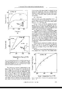
High Aspect Ratio Microstructures in LiNbO3 Produced by Ion Beam Enhanced Etching Frank Schrempel1, Thomas Gischkat1, Holger Hartung2, Ernst-Bernhard Kley2, Werner Wesch1, Andreas Tünnermann2 1 Institut für Festkörperphysik 2 Institut für Angewandte Physik Friedrich-Schiller-Universität Jena, Max-Wien-Platz 1, D-07743 Jena, Germany ABSTRACT This work presents data on damage evolution, volume expansion and etching behavior of LiNbO3 irradiated with Ar+-ions as a function of irradiation and etching conditions. Single crystals of x- and z-cut LiNbO3 were irradiated at room temperature and 15 K using Ar-ions with energies between 60 and 600 keV and ion fluences between 5 x 10¹² and 1 x 1015 cm-2. The damage formation investigated with RBS channeling analysis depends on the crystal cut as well as on the irradiation temperature. Irradiation of z-cut material at 300 K causes complete amorphization at 0.4 dpa (displacements per target atom). In contrast 0.27 dpa are sufficient to amorphize the xcut LiNbO3. Irradiation at 15 K reduces the number of displacements per atom necessary for amorphization to 0.18 dpa. To study the etching behavior ~500 nm thick amorphous layers were generated via multiple irradiations with Ar+-ions. Etching was performed in HF-solution of different concentration and at different temperatures. The influence of the irradiation and etching conditions on damage formation and etching of LiNbO3 is discussed. In conclusion, negligible etching of the perfect crystal, high etching rates and high contrast of Ion Beam Enhanced Etching (IBEE) allow the realization of high aspect ratio microstructures in LiNbO3.
INTRODUCTION High aspect ratio micro- and nanostructures in electro-optical materials are of great interest due to the possibility to create ridge waveguides and crystals with photonic band gap structures. LiNbO3 (lithium niobate) is an important electro-optical material widely used for the fabrication of integrated optical devices because it possesses large electro-optical, piezoelectric and nonlinear optical coefficients. In order to create photonic crystals in LiNbO3, the material has to be removed periodically with dimensions in the order of the magnitude of the wavelength. But the achievement of nanometric structures in LiNbO3 is a challenging problem, because the material is very resistant to standard etching technologies. Therefore, a series of alternative technologies such as reactive ion etching (RIE) [1], ion beam etching with inert and reactive ions (IBE, RIBE) [2], sputtering with focused ion beams (FIB) [3,4] as well as wet chemical etching after ferroelectric domain inversion [5], ion exchange [6-8] and ion irradiation (IBEE: Ion Beam Enhanced Etching) [9-14] have been investigated and applied to pattern LiNbO3. Among these techniques the latter is most promising, because it has high selectivity, independence of the crystal symmetry and short production times. Multiple implantation with different energies and fluences can be used to obtain deep structures with smooth botto
Data Loading...