Improvement of LDI BUMP Stripping Process by Development of Room Temperature PR Stripper
- PDF / 350,764 Bytes
- 7 Pages / 612 x 792 pts (letter) Page_size
- 11 Downloads / 336 Views
0990-B07-16
Improvement of LDI BUMP Stripping Process by Development of Room Temperature PR Stripper Young- Sam Lim1, Dong Chan Bae2, Hyun-Joon Kim1, Young- Nam Kim1, Young Ho Kim1, and Tae Sung Kim1 1
Manufacturing Technology Team1, Samsung Electronics, San#24 Nongseo-Dong,Giheung-Gu, Young-City, 446-711, Korea, Republic of 2
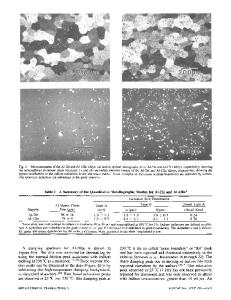
BUMP Group, Samsung Electronics, San#24 Nongseo-Dong,Giheung-Gu, Young-City, 446-711, Korea, Republic of ABSTRACT Bump process using gold bump leads to many cleaning problems like polymer residues, metal and polyimide consumption after stripping process. First of all, stripping process of bump photoresist is very difficult. Because the thickness of PR pattern of bump is thicker than that of general metal line at least 100 times. The improvement of LDI Bump stripping process was obtained by new chemical. Additive plays critical role in changing wettability which is important factor for improving stripping ability. It was found that new chemical was superior to the commercial chemical in terms of chemical stability, removal efficiency of polymer residue and the decrease rate in metal and polyimide consumption. Also, the removal mechanism of photoresist pattern was investigated by measured Raman equipment. Enhancement of yield in mass production line of semiconductor was obtained by new chemical. INTRODUCTION In order to process display data for the implementation of various moving pictures, Liquid crystal displays driver integrated circuit (LDI) devices have been currently used in mobile phone, PDA and TFT LCD Panel. Among the manufacturing processes of LDI devices, Bump process plays essential roles in facilitating connection of a packaged semiconductor chip having multiple pins on a printed circuit board of LCD panel [1, 2]. Bump process leads to many stripping problems like polymer remnants, metal and polyimide consumption after stripping process. First of all, stripping process of bump photoresist is one of the difficult technologies since thickness of photoresist pattern of bump is thicker than that of general metal line at least 100 times [3]. So, the bottom portion of the photoreist may not be removed in a stripping process, thereby inducing a failure of the semiconductor device [4].
Most organic strippers recently used for removing the photoresist which is forming the bump electrode are not satisfied in terms of removal efficiency and readsorption of photoresist residues on the bump electrodes [5]. So, double cleaning process or high temperature conditions at 50 to 130 oC are normally performed. But these bump process increases processing time and high thermal budget. Moreover, chemical vapors are generated, due to the high temperature, which contaminates the cleanroom air. In this study, we reported the improvement of LDI BUMP stripping process at 25 oC with new chemical. Furthermore, the result of yield enhancement was identified in mass production line. EXPERIMENTAL The commercial chemical for bump process was obtained from local company. Our stripping chemicals were composed for
Data Loading...