Inhibited SN Surface Segregation in Epitaxial SN x GE 1-x Alloy Films Grown by Pulsed Laser Deposition
- PDF / 963,146 Bytes
- 6 Pages / 414.72 x 648 pts Page_size
- 98 Downloads / 322 Views
ALLOY
M.E. Taylor, G. He, C. Saipetch, and H.A. Atwater Thomas J. Watson Laboratories of Applied Physics California Institute of Technology, Pasadena, CA 91125
ABSTRACT Epitaxial and compositionally homogeneous SnGel-.i alloy films have been grown on Si (001) by pulsed laser deposition using elemental Sn and Ge targets. These results demonstrate that pulsed laser deposition can be used to grow alloys by overcoming the strong tendency for Sn surface segregation seen in growth by other methods such as molecular beam epitaxy.
INTRODUCTION Electronic structure calculations predict that the binary alloy Sn.Gel_= is a direct gap semiconductor with a band gap that ranges between 0.55 eV and 0 eV as the composition is varied between x=0.2 and x=0.8, as shown in Figure 1 [1]. Significantly, SnrGel_= also has potential for monolithic integration on Si substrates. As a result, Sn.Gel-i is of interest for future Si-based infrared optoelectronics applications. The synthesis of Sn.,Gel_= alloy films has been the subject of many previous investigations, most of which relied on molecular beam epitaxy [2, 3, 4, 5, 6], sputtering [7], or solid phase recrystallization [8, 9, 10] as the growth method. These methods have not as of yet produced crystalline films in the desired composition range. This lack of success is due primarily to the segregation of Sn to the surface of the growing film. The tendency for Sn surface segregation results from two competing kinetic processes [11, 12]. During steady-state growth, the surface layer is transformed into a bulk layer. Since the bulk equilibrium Sn composition is smaller than the Sn composition of the flux, Sn segregates to the surface. The time available for segregation from the bulk to the surface is limited by the film growth rate. The Sn incorporation coefficient is a strong function of a Peclet number that expresses the ratio of the growth rate to the rate of segregation by diffusion between bulk and surface layers. Deposition methods with high Peclet numbers are predicted to produce films with high incorporation coefficients. Pulsed laser deposition (PLD) has been used previously to deposit crystalline semiconductor films [13, 14]. PLD differs from more conventional growth methods in that it is characterized by high growth rates and high mean particle energies. In light of the assumptions made concerning the kinetics of Sn surface segregation, PLD is a potentially useful method for synthesizing Sn.Gel-..f films.
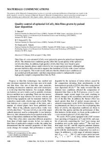
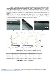
SN.GE 1_. FILM GROWTH BY PULSED LASER DEPOSITION Films were grown in a loadlocked PLD chamber equipped with reflection high energy electron diffraction (RHEED). The target consisted of a polycrystalline Ge (99.999%) wafer overlaid with pie-shaped wedges of Sn (99.9999%) that covered approximately 55% of the surface. The target was rotated at 10 rpm to ensure an average flux composition value of 0.55 and to avoid severe erosion of the target in any particular area. Test-grade Si (001) substrates were cleaned by 97 Mat. Res. Soc. Symp. Proc. Vol. 388 0 1 99 5 Materials Resear
Data Loading...