Lattice-Matched InAsN(X=0.38) on GaAs Grown by Molecular Beam Epitaxy
- PDF / 833,601 Bytes
- 6 Pages / 414.72 x 648 pts Page_size
- 31 Downloads / 413 Views
ABSTRACT In this paper, we report the MBE growth of high nitrogen content lattice-matched InAs1 _xNx (x=0.38) single crystal epitaxial films on GaAs. The nitrogen incorporation is about an order higher than previously reported on other mixed group V nitride alloys. These data are consistent with a nitrogen solubility limit calculation in various III-V binary alloys, which predicts orders of magnitude higher nitrogen incorporation in InAs than any other alloys. InAsN growths were obtained using a modified ECR-MBE system with atomic-nitrogen generated by an ECR plasma source. Improved crystal quality was obtained using a "template" growth technique. An x-ray linewidth of 270 arc-s was achieved on a 0.4 .trm thick InAs0 .62No.38/GaAs multi-layer structure. Hall effect data show these InAsN films are semi-metallic. INTRODUCTION Recently, the growth of mixed group V nitride alloy III-V compound semiconductors has gained interest [1-31. This increased interest in nitride-based semiconductors is primarily related to the potential applications in short wavelength (blue and violet) emitting devices and the capability of growing arsenide nitride and phosphide nitride lattice-matched to silicon [2]. The potential of combining the direct bandgap materials on a Si substrate is attractive for Si-based bandgap engineering applications such as base layers inHBTs, channel layers in FETs, low 10
1
8
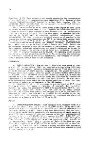
.AIN,x
6
1
AIN
C2
GaN, \aN o_. 2\\":>_.InN
Al. p
a.. AlAs Al•AAs,X AI.AAS
a SIC a
0
-4
4
4.5
5 5.5 Lattice constant (Angstrom)
InAs
6
6.5
Fig. 1 Estimated bandgap versus lattice constant for the ternaries of the InGaAIAsPN material system. The solid lines represent empirical extrapolation from low nitrogen content alloys for the direct bandgap, while the dashed lines represent the X-point. The point Fam is the ab initio theoretical prediction for the bandgap of famatinite GaASb.75N0 .25 .
335
Mat. Res. Soc. Symp. Proc. Vol. 423 01996 Materials Research Society
ohmic contact layers, and quantum well layers for resonant tunneling devices. Figure 1 shows the estimated bandgap versus lattice constant for the ternaries of the InGaAIAsPN material system [4]. The solid lines represent empirical extrapolation from low nitrogen content alloys for the direct bandgap, while the dashed lines represent the X-point. A bowing coefficient in GaAsN (18 eV) for arsenide nitride and in GaPN (14 eV) for phosphide nitride were used in the calculation. The point labeled Fam represents an ab initio estimate from famatinite ordered GaAso.75No.25with a predicted bandgap of about I eV, indicating that some of the intermediate alloys may have finite bandgaps contrary to the low nitrogen quadratic extrapolation. The major challenge in growing the group IlI-V-nitride alloy compounds results from the large difference in the atomic radii of nitrogen and the other group V elements. Such material systems with large differences in atomic radii are known to have large miscibility gaps and cannot be grown by equilibrium techniques [5]. However, immi
Data Loading...