Mechanism for LiNb 3 O 8 phase formation during thermal annealing of crystalline and amorphous LiNbO 3 thin films
- PDF / 543,868 Bytes
- 11 Pages / 585 x 783 pts Page_size
- 84 Downloads / 311 Views
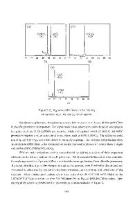
The kinetics of second phase formation during the thermal annealing of crystalline and amorphous LiNbO3 (LN) thin films was investigated. When c-axis-oriented LN texture film was annealed at temperatures higher than 700 °C, Li2O desorbed from the surface and grain boundaries, which induced epitaxial precipitation of the LiNb3O8 phase on the LN (0001) plane. While the LiNb3O8 volume exhibited saturation behavior against annealing time, oxygen atoms continued to diffuse out from the inner part of the film. Arrhenius plots of the rate of LiNb3O8 formation and oxygen loss were scaled with common activation energy of 30.5 kcal/mol. In terms of phase formation from amorphous LN, annealing at 700 °C in a vacuum induced rapid crystallization into mixtures of LN and LiNb3O8, the volume ratio of which can be explained by the phase separation model. Annealing in an O2 atmosphere, however, produced an incubation time before crystallization and a larger volume fraction of LiNb3O8 after crystallization. Oxygen molecules that penetrated into the film will hinder the migration of atoms and decelerate crystallization. Vacancies produced as a result of Li2O loss will facilitate the nucleation of LN and LiNb3O8 pairs while maintaining the epitaxial relation.
I. INTRODUCTION
LiNbO3 (LN) crystal is a key substance that is absolutely necessary in quantum optoelectronics. Thanks to its large electro-optic effect, high-frequency modulators and optical switches are now in the production stage. Other emerging applications include frequency-doubled lasers and wavelength converters that exploit the nonlinear effect. These functional devices normally feature diffusive waveguides formed on high-quality single crystals grown from melts. Replacing bulk crystal with thin films, however, opens the way to easily fabricating spacelimiting waveguides with large differences in the refractive indices of core and cladding layers. In recent years, we demonstrated the formation of highly c-axis-oriented polycrystalline LN texture films by electron–cyclotron– resonance (ECR) plasma sputtering on representative materials used for semiconductor technologies, such as Si,1 SiO2,2 TiN,3,4 and indium–tin oxide.4 These systems provide the basis for fabricating integrated photonic devices on a wafer.5–7 Possible target devices are compact frequency modulators, ultrasensitive electric field sensors, and light deflectors. Periodically poled LN on silicon-on-insulator substrates as well as twoa)
Address all correspondence to this author. e-mail: [email protected] DOI: 10.1557/JMR.2007.0208 1726
J. Mater. Res., Vol. 22, No. 6, Jun 2007
dimensional slab waveguides comprising secondharmonic generation and photonic band-gap structure seem to be promising applications in combination with silicon microphotonics. Although employing thin films has the potential for dramatically reducing the production cost of devices, marginal performance in electro-optic and waveguiding loss properties is a drawback.8 One serious problem specific to LN is the precipitation of the s
Data Loading...