Multi-Color Quantum Well Infrared Photodetectors for Mid-, Long-, and Very Long- Wavelength Infrared Applications (invit
- PDF / 624,079 Bytes
- 12 Pages / 612 x 792 pts (letter) Page_size
- 8 Downloads / 323 Views
Multi-Color Quantum Well Infrared Photodetectors for Mid-, Long-, and Very Long- Wavelength Infrared Applications (invited) Sheng S. Li Department of Electrical and Computer Engineering University of Florida, Gainesville, FL 32611 Email address: [email protected]
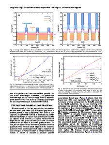
ABSTRACT Quantum well infrared photodetectors (QWIPs) have been widely investigated for the 3-5 µm mid-wavelength infrared (MWIR) and 8-12 µm long-wavelength infrared (LWIR) atmospheric spectral windows as well as very long wavelength infrared (VLWIR: λc > 14 µm) detection in the past decade. The mature III-V compound semiconductor growth technology and the design flexibility of device structures have led to the rapid development of various QWIP structures for infrared focal plane arrays (FPAs) applications. In addition to the single-color QWIP with narrow bandwidth, the multi-color QWIP required for advanced IR sensing and imaging applications have also been emerged in recent years. Using band gap engineering approach, the multi-color (2, 3, and 4- color) QWIPs using multi-stack quantum wells with different well width and depth and voltage-tunable triple- coupled quantum well (TCQW) structure for detection in the MWIR, LWIR, and VLWIR bands have been demonstrated. In this paper, the design, fabrication, and characterization of a voltage-tunable 2-stack 3-color QWIP for MW/LW/LW IR detection and a 3-stack 3-color QWIP for detection in the water, ozone, and CO2 atmospheric blocking bands are depicted.
1. INTRODUCTION Recent advances in III-V semiconductor epitaxial layer growth techniques such as molecular beam epitaxy (MBE) [1] and metalorganic chemical vapor deposition (MOCVD) have made it possible to grow a wide variety of novel semiconductor heterostructures. Significant progress has been made in quantum wells and superlattice optoelectronic devices using these growth techniques. The quantum well is formed by using an ultra thin layer of narrow band gap semiconductor (e.g., GaAs) sandwiched between two thin wider band gap semiconductor (e.g., AlGaAs) barrier layers. The motion of the carriers perpendicular to the layers becomes quantized so that localized two-dimensional subbands of quantized states are formed inside the quantum well. [2] Early proposals of using optical intersubband transitions in quantum wells for IR detection were made by Chang et al. [3], Esaki, Tsu, and Sakaki[4-5], and Coon and Karunasiri [6]. The intersubband absorption in GaAs quantum wells was first observed by West and Eglash [7] and followed by Harwit and Harris [8]. Levine et al. [9] demonstrated the first GaAs QWIP in 1987. Since then, QWIPs based on the bound-tobound (B-B), bound-to-continuum (B-C) [10], and bound-to-miniband (B-M) [11]transitions have been widely investigated for the 3 to 5 µm mid-wavelength infrared H4.1.1
(MWIR) and 8 to 14 µm long-wavelength infrared (LWIR) detection [12-13]. Additionally, there is a considerable interest in the development of multi-stack and voltage- tunable asymmetrical coupled quantum well structures for multi-color focal plane
Data Loading...