Optical Demultiplexer Device: Frequency and optical bias analysis
- PDF / 647,308 Bytes
- 6 Pages / 432 x 648 pts Page_size
- 82 Downloads / 352 Views
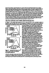
Optical Demultiplexer Device: Frequency and optical bias analysis P. Louro1,2, M. Vieira1,2,3, M. A. Vieira1,2, T. Silva1 1 Electronics Telecommunications and Computer Dept, ISEL, Lisbon, Portugal. 2 CTS-UNINOVA, Lisbon, Portugal. 3 DEE-FCT-UNL, Quinta da Torre, Monte da Caparica, 2829-516, Caparica, Portugal ABSTRACT In this paper we present results on the use of a multilayered a-SiC:H heterostructure as a device for wavelength-division demultiplexing of optical signals. This device is useful in optical communications applications that use the wavelength division multiplexing technique to encode multiple signals into the same transmission medium. The device is composed of two stacked p-i-n photodiodes, both optimized for the selective collection of photo generated carriers. Band gap engineering was used to adjust the photogeneration and recombination rates profiles of the intrinsic absorber regions of each photodiode to short and long wavelength absorption and carrier collection in the visible spectrum. The photocurrent signal using different input optical channels was analyzed at reverse and forward bias and under steady state illumination. A demux algorithm based on the voltage controlled sensitivity of the device was proposed and tested. The operation frequency of the device was analyzed under different optical bias conditions. An electrical model of the WDM device is presented and supported by the solution of the respective circuit equations. INTRODUCTION Wavelength division multiplexing (WDM) devices are used when different optical signals are encoded in the same optical transmission path, in order to enhance the transmission capacity and the application flexibility of optical communication and sensor systems. The use of WDM technologies not only provides high speed optical communication links, but also offers advantages such as higher data rates, format transparency, and self-routing. Various types of available WDM devices include prisms, interference filters, and diffraction gratings. Currently modern optical networks use Arrayed Waveguide Grating (AWG) as optical wavelength (de)multiplexers [1] that use multiple waveguides to carry the optical signals. In this paper we report the use of a monolithic WDM device based on an a-Si:H/a-SiC:H multilayered semiconductor heterostructure. The device makes use of the fact that the optical absorption of the different wavelengths can be tuned by means of electrical bias changes or optical bias variations. This capability was obtained using adequate engineering design of the multiple layers thickness, absorption coefficient and dark conductivities [2]. DEVICE CONFIGURATION The device described herein operates from 400 to 700 nm which makes it suitable for operation at visible wavelengths in optical communication applications. The device is a multilayered heterostructure based on a-Si:H and a-SiC:H. The configuration of the device includes two stacked p-i-n structures between two electrical and transparent contacts (Fig. 1). Both front (pin1) and back (pin2) structures a
Data Loading...