Optical study of SiGe films grown with low temperature Si buffer
- PDF / 88,629 Bytes
- 6 Pages / 612 x 792 pts (letter) Page_size
- 18 Downloads / 231 Views
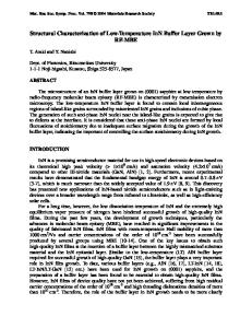
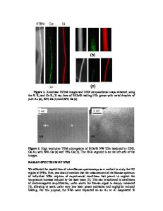
Optical study of SiGe films grown with low temperature Si buffer Y. H. Luo, J. Wan, J. L. Liu, and K. L. Wang Device Research Laboratory, Department of Electrical Engineering, University of California at Los Angeles, Los Angeles, CA 90095-1594 ABSTRACT In this work, SiGe films on low temperature Si buffer layers were grown by solid-source molecular beam epitaxy and characterized by atomic force microscope, photoluminescence and Raman spectroscopy. Effects of the growth temperature and the thickness of the low temperature Si buffer were studied. It was demonstrated that using proper growth conditions of the low temperature Si buffer, the Si buffer became tensily strained and gave rise to the compliant effect. High-quality SiGe films with low threading dislocation density have been obtained. INTRODUCTION High-quality strain-relaxed SiGe buffer layers have been widely used as “virtual substrates” for the growth of strain Si/SiGe high electron mobility transistors and metal-oxidesemiconductor field effect transistors [1,2], and Ge photodiodes on Si [3]. However, the large lattice mismatch (~ 4.17%) between Si and Ge usually results in lots of threading dislocations in SiGe buffer layers, which propagate through the SiGe buffer layer into the active layers and deteriorate the device performance [4]. Several methods have been used to grow high quality strain-relaxed SiGe, such as graded composition [5], compliant substrate [6], etc. Recent reports indicated that the use of low-temperature (LT) buffer layers could significantly reduce threading dislocation density in the SiGe layer [7]. It was believed that the LT Si layer plays important roles: provides low energy sites for dislocation nucleation, or point defects for trapping of propagating dislocations, and contain the mismatch strain [8]. In this work, photoluminescence (PL) and Raman spectroscopy were used to study the strain and dislocations of the relaxed SiGe films grown on low temperature Si buffer. EXPERIMENTAL DETAILS The samples investigated were grown by solid source molecular beam epitaxy (MBE) in a Perkin-Elmer system. A P- type Si (001) substrate was cleaned by using a modified Shiraki method and loaded into the MBE system after a diluted HF dip. At first, a 60 nm Si buffer was grown at 600 o C to reduce the defects and smooth the surface of the substrate. After the growth of a followed-up LT Si layer, a SiGe layer was grown at 480oC. The growth rate for both the Si layer and the SiGe layer were about 1Å/s. PL was measured at 4.5 K using an Ar+ 488 nm laser line. Raman spectra were taken using a 457.9 nm Ar+ laser line. Two series of samples were studied in this paper. Series A is 150 nm Si0.8Ge0.2 films grown on 200 nm LT Si buffer layer with different growth temperatures, which was used to optimize the growth temperature of the LT Si buffer layer. Series B is 200 nm Si0.8Ge0.2 films P3.11.1
grown on 400oC LT Si layer with different thickness, which was used to optimize the thickness of the LT Si buffer layer. RESULTS AND DISCUSSION
D1/D2 Peak area (a.
Data Loading...