PbO-sensitized ZnO nanorod arrays for enhanced visible-light-driven photoelectrochemical performance
- PDF / 681,783 Bytes
- 9 Pages / 584.957 x 782.986 pts Page_size
- 46 Downloads / 1,045 Views
semiconductor system for solar-energy utilization by photoelectrochemical (PEC) water splitting, the effective absorption of visible light and the efficient separation and transfer of photogenerated charge carriers are still of key importance. In this manuscript, composite photoanodes of PbO sensitized ZnO nanorod arrays were prepared by a two-step hydrothermal process and used as anodes for PEC test under visible-light irradiation. The photocurrent achieved the highest value of 94 lA cm 2 at 0.8 V (versus Ag/AgCl electrode) when the amount of Pb source was optimized to form only a thin layer (a few nanometers) of PbO nanoparticles on the surfaces of ZnO nanorods. Such a nanostructure enabled the visible-light absorption, and also ensured the sufficient contact of PbO with ZnO to form junction with a type II band alignment and the sufficient contact with aqueous solution to form interfaces, thus facilitating the excitation, separation, and transfer of charge carriers to generate photocurrent and finally enhancing the PEC activity.
I. INTRODUCTION
ZnO is a widely used semiconductor material in various aspects of solar energy utilization due to its thermal stability, low cost, nontoxicity, and easily controlled morphology.1–4 ZnO has a bandgap of 3.3 eV, which means only ultraviolet (UV) light can be harvested. Many attempts have been carried out to extend the light-absorption range, such as doping with alien metal cations and/or nonmetal ions,5–7 or sensitizing with organic dyes8,9 or with narrower-bandgap semiconductor quantum dots.10–12 Moreover, lots of work has been done to enhance the transfer of photogenerated charge carriers so as to reduce the consumption in radiative combination.13,14 It has been proved to be a promising way to expand the light response and meanwhile to strengthen the separation of photogenerated electron–hole pairs by sensitizing wide-bandgap semiconductor with narrowerbandgap semiconductor.15–17 Aligned one-dimensional semiconductor photoelectrodes were also demonstrated to be very beneficial to the transfer of photogenerated charge carriers due to the direct pathway without resistance of crystal boundary.18–20 PbO, as a heavy oxide, is comprehensively investigated as an additive in glass material to change the electronic and nonlinear optical properties.21,22 Iwaszuk Contributing Editor: Heli Wang Address all correspondence to these authors. a) e-mail: [email protected] b) e-mail: [email protected] DOI: 10.1557/jmr.2016.150 J. Mater. Res., 2016
et al. presented a first-principles density functional theory (DFT) investigation on TiO2 modified with PbO and PbO2 nanoclusters, which strongly were adsorbed on all TiO2 surfaces to create new Pb–O and Ti–O interfacial bonds.23 PbO modified TiO2 introduced new states above the valence band (VB) of TiO2 and therefore resulted in a shift of the band onset into the visible-light region, while PbO2 modified TiO2 resulted in visible-light-driven photocatalysis via new states just below the conduction band (CB) of TiO2. Bhachu et al. reported
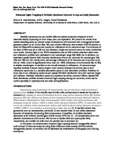
Data Loading...