Preparation and properties of ferroelectric Bi 2 SrTa 2 O 9 thin films for FeRAM using Flash-MOCVD
- PDF / 3,459,949 Bytes
- 6 Pages / 414.72 x 648 pts Page_size
- 62 Downloads / 259 Views
mixed solution with an appropriate ratio in the
-.. ,
mixing manifold was introduced into the vaporizer by the liquid injection pump. The inside of the vaporizer was kept at 200 V and
Fig. I Shematic diagram of the MOCVD system 195
Mat. Res. Soc. Symp. Proc. Vol. 415 01996 Materials Research Society
evacuated at a pressure between 0. 1 torr and 20 torr. The vaporized gases were transported by Ar carrier gas into the quartz reactor and mixed with 02 which were then introduced Pt/Ti/SiO 2/Si(100) Substrate directly into the reactor. Typical growth 500 - 700 oC Substrate temperature conditions are presented in Table I. 0.2 - 10 torr System pressure Films deposited were annealed at 8(W) 900 - 1800 sccm Ar/O2 gas flow rates VCin flowing oxygen (-2 /min.) for an hour. 20-70 % Partial pressure of 02 In order to characterize the electrical properties, 15 - 20 min Growth time 2(X) nm Pt top electrodes were evaporated on post annealed films using patterned masks. The size of round upper electrodes were 200 gtm in diameter. Compositions of films prepared were characterized by electron probe micro analysis (EPMA). X-ray diffraction (XRD) with a fixed incident angle of 5' was performed to investigate the crystal structures. More detailed crystallographic aspects were analyzed by transmission electron microscopy. Surface morphologies were observed by atomic force microscopy (AFM) and field emission scanning electron microscope (FE-SEM). Electrical properties were characterized using the Radiant Technology RT66A test system.
Table I. The typical growth conditions for MOCVD Bi 2 SrTa 2O9 thin films
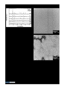
3. Results and discussion 3.1 Crystal structure of as-deposited films An XRD pattern from the asdeposited films grown with typical CVD conditions (6W) VC,10 torr) is shown in figure 2. It was successfully indexed assuming a fluorite-type structure (space group : Fm3m; illustrated in the inset) with a lattice parameter of a=5.446A, and this assumption was supported by results of TEM observation. Figure 3 (a) shows a bright field image of the as-deposited film. The grains are spherical in shape and are estimated to be around 50 - 1M nm in diameter. A selected area electron diffraction (SAED) pattern of the as-deposited film is shown in figure 3 (b). All of the diffraction spots are explained by the fluoritetype structure with a space group of Fm3m.
2 0 [(dg.] Fig.2 An XRD pattern of the as-deposited films grown with the typical CVD conditions
qt ýT%
Fig.3 A bright field image ((a); left) and a SAED pattern ((b); right) of the as-deposited film 196
3.2 Crystal structure and surface morphology of post-annealed films Figure 4 displays an XRD pattern from a film grown with the typical CVD conditions and annealed at 8W0 CCin an oxygen flow (2 l/min.) for 1 hour. The vertical tick marks indicate the expected peak locations assuming a simplified model with a space group of Fmmm (illustrated in the inset). It turned out that the main phase was randomly oriented Bi2SrTa2O) with small 0 C a secondary phase which will be amount M discus
Data Loading...


