Preparation of Ge 2 Sb 2 Te 5 Thin Film for Phase Change Random Access Memory by RF Magnetron Sputtering and DC Magnetro
- PDF / 282,507 Bytes
- 6 Pages / 612 x 792 pts (letter) Page_size
- 104 Downloads / 266 Views
0918-H07-10-G08-10
Preparation of Ge2Sb2Te5 Thin Film for Phase Change Random Access Memory by RF Magnetron Sputtering and DC Magnetron Sputtering Shin Kikuchi, Dong Yong Oh, Isao Kimura, Yutaka Nishioka, and Koukou Suu Institute for Semiconductor Technologies, ULVAC,inc., 1220-1,Suyama, Susono, Shizuoka, 410-1231, Japan
ABSTRACT Ge2Sb2T5 (GST) thin films were prepared by RF magnetron sputtering and DC magnetron sputtering on a SiO2/Si (100) substrate. The composition of the DC sputtered GST films, contained less Te than the target composition, while the composition of RF sputtered GST films were almost the same as the target composition. The RF sputtered GST films were hcp crystals after 400℃ annealing. On the other hand, the DC sputtered films were mixed-phase of fcc and hcp. The resistivity of DC Sputtered GST films was higher than the RF sputtered film because of poor crystallinity. The uniformity of RF sputtered film was better than the DC sputtered film. Key words; GST; RF magnetron sputtering; DC magnetron sputtering; resistivity INTRODUCTION Phase Change Random Access Memory (PRAM) is a promising candidate for nonvolatile memories required in the next generation because of its non-volatility, good scalability, fast read and write times, strong cycling performance, and excellent compatibility with current CMOS logic processes. [1] PRAM uses the reversible phase change of a calcogenide material (for example Ge2Sb2T5-GST), which shows two difference phases, such as a crystalline one for the set state with low resistance and an amorphous one for the reset state with high resistance. [2] It is reported that the crystallization speed of GST greatly depends on the composition of the GST film.[3] In this work, we investigate the difference in character of the GST as a function of various sputtering methods. Good controllability of the composition and good uniformity of resistance of the GST thin film is obtained by RF magnetron sputtering. EXPERIMENT
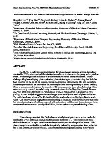
A multi-chamber sputtering system ULVAC CERAUS ZX-1000PVD (Figure 1) was used for GST deposition on φ200mm SiO2/Si substrates. GST films were deposited at R.T. by RF magnetron sputtering and DC magnetron sputtering with a φ300mm sintered target. The GST deposition conditions are shown in Table.1. As-deposited GST films were amorphous. Crystallization was performed at temperatures above 400℃ for 10min in N2 ambient. XRD
analysis was used to determine the crystallized phase, and XRF analysis was used to evaluate the composition of the films. The Sheet resistances of the GST films are measured by Omnimap RS100 (KLA tencore). A test phase-change device was fabricated by the process shown in Figure 2. The fabricated device was reversibly switched between crystalline (set) and amorphous (reset) phases using a pulse generator. The voltage pulse varial from 2.0V to 10.0V for reset operations, while the pulse width was 100 nsec.
Heater
RF
RF :wafer
DC
DC
L/UL Chamber L/UL chamber
Auto-loader
Wafer aligner
Figure 1. Schematic diagram of CERAUS ZX-1000 PVD. Table.1.
Data Loading...