Role of Pb 2+ Adsorbents on the Opto-Electronic Properties of a CsPbBr 3 Nanocrystal: A DFT Study
- PDF / 592,155 Bytes
- 8 Pages / 432 x 648 pts Page_size
- 47 Downloads / 277 Views
MRS Advances © 2019 Materials Research Society DOI: 10.1557/adv.2019.268
Role of Pb2+ Adsorbents on the Opto-Electronic Properties of a CsPbBr3 Nanocrystal: A DFT Study Aaron Forde1, Erik Hobbie1, Dmitri Kilin2 1 Department of Materials Science and Nanotechnology, North Dakota State University, Fargo, North Dakota 58102, United States
2 Department of Chemistry and Biochemistry, North Dakota State University, Fargo, North Dakota 58102, United States
ABSTRACT
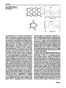
Fully inorganic lead halide perovskite nanocrystals (NCs) are of interest for photovoltaic and light emitting devices due to optoelectronic properties. Understanding the surface chemistry of these materials is of importance as surface defects can introduce trap-states which reduce their functionality. Here we use Density Functional Theory (DFT) to model surface defects introduced by Pb2+ on a CsPbBr3 NC atomistic model. Two types of defects are studied: (i) an under-coordinated Pb2+ surface atom and (ii) Pb2+ atomic or molecular adsorbents to the NC surface. From the DFT calculations we compute the density of states (DOS) and absorption spectra of the defect models to the pristine fully-passivated NC model. We observe that for the low surface defect regime explored here that neither (i) or (ii) produce trap-states inside of the bandgap and exhibit bright optical absorption for the lowest energy transition. From the models studied, it was found that the Pb2+ atomic absorbent provides broadening of the conduction band edge, which implies chemisorption of Pb2+ to the NC surface. At higher defect densities it would be expected that Pb2+ atomic absorbents would introduce trap-states and degrade the opto-electronic properties of these materials.
INTRODUCTION CsPbX3 (X=Cl,Br,I)perovskite nanocrystals (NCs) have become popular materials for optoelectronics due to their photo-physical properties, such as tuneable light emission, high photoluminescence quantum yields (PLQYs), and fast radiative lifetimes[1]. Photo-excited electrons and holes in a CsPbX3 NC are physical manifestations of ‘particles in a box’ which promotes fast and efficient radiative
1981
Downloaded from https://www.cambridge.org/core. Uppsala Universitetsbibliotek, on 25 Jan 2020 at 10:57:55, subject to the Cambridge Core terms of use, available at https://www.cambridge.org/core/terms. https://doi.org/10.1557/adv.2019.268
recombination due to spatial confinement within the NC. A general heuristic for semiconductor NCs is that they require complete surface passivation to satiate undercoordinated atoms at the NC surface. Undercoordinated surface atoms can create electronic states inside of the intrinsic bandgap which promotes non-radiative recombination pathways by localizing charge density on the surface of the NC which reduces PLQY[2]. With perovskites having a mixed ionic-covalent bonded crystal structure their surface chemistry reflect the same feature. CsPbX 3 NCs can have two types of surface termination: Cs-X and Pb-X. It has been generally found that two counter ligands are needed to passi
Data Loading...