Sb-Doped Polycrystalline Si Obtained by Means of Sb and Si Thin-Film Reactions
- PDF / 1,940,116 Bytes
- 6 Pages / 420.48 x 639 pts Page_size
- 3 Downloads / 329 Views
Sb-DOPED POLYCRYSTALLINE Si OBTAINED BY MEANS OF Sb AND Si THIN-FILM REACTIONS S.F. Gong, A.E. Robertsson,
S.-E. Hbrnstrbm,
G. Radnoczi*,
and
H.T.G. Hentzell, Department of Physics and Measurement Technology Link6ping University, S-581 83 Link6ping, Sweden *Permanent address: Research Institute for Technical Physics Hungarian Academy of Sciences, Budapest IV, Foti Ut 56, Hungary
of
the
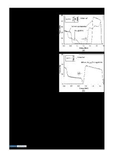
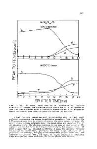
ABSTRACT We have grown Sb-doped poly-Si by thin-film reactions between Sb and amorphous Si (a-Si). The reactions and microstructures of the films were during in situ investigated by transmission electron microscopy (TEM) The reactions either annealing and Auger electron spectroscopy (AES). resulted in an amorphous Sb-Si (a-Sb-Si) alloy or caused crystallization of a-Si at low temperatures, depending on the film thickness of the a-Si layer as well as the heating rate. The electrical properties of the as-deposited and the annealed thin multi-layers deposited on Si0 2 layer were determined using Hall measurements. After annealing at 1375 K for 60 minutes, Sb-doped poly-Si with a resistivity of 1.4x10⁻² ohm-cm was obtained. A p-n junction was formed in a p-type Si substrate by using an a-Si/Sb/a-Si multi-layer as a diffusion source. The doping concentration in the Si substrate was obtained using secondary ion mass spectrometry (SIMS). I. INTRODUCTION Polycrystalline silicon (poly-Si) with various doping levels has important applications in monolithic semiconductor circuits. Further, highly doped poly-Si can be used as a diffusion source for the formation of p-n junctions in single crystal Si [1-6]. There investigations have been stimulated by the growing interest in bipolar transistors with poly-Si emitters and in MOS devices with contact diffusion as well as in the improvement of solar cells. Poly-Si films are conventionally deposited in a vapor deposition (CVD) process by pyrolyzing silane at a chemical temperature of about 925 K without dopants. The doping elements, usually P, As, or B are subsequently added by thermal diffusion, sometimes combined with ion implantation. In this paper, however, we present an Sb-doped polySi which resulted from solid-state reactions between Sb and Si thin films obtained by electron-beam evaporation. Because a high concentration of Sb could be achieved in the poly-Si using this method, the resulting Sb-doped poly-Si is supposed to be a good diffusion source for doping of the Si substrate. In the present work, by using TEM, AES, SIMS, and Hall measurements, we have investigated solid-state reactions between Sb and Si thin films, and microstructures and electrical properties of the resulted Sb-doped poly-Si. Moreover, a p-n junction was formed in a p-type Si substrate by using the a-Si/Sb/a-Si multi-layer as a diffusion source. Cross-section TEM illustrates the structure of the resulted layer on the Si substrate and the interface between the top layer and the Si substrate. The Sb doping profile in the Si substrate was obtained by SIMS measurements. II.
EXPERIMENTAL DETAILS Thin
film
structures
Data Loading...