Simulation of DC Characteristics of Nano-Scale Hydrogen-Terminated Diamond MISFETs
- PDF / 773,024 Bytes
- 6 Pages / 612 x 792 pts (letter) Page_size
- 57 Downloads / 262 Views
Simulation of DC Characteristics of Nano-Scale Hydrogen-Terminated Diamond MISFETs Xi Zhou, Frances Williams and Sacharia Albin Department of Engineering, Norfolk State University Norfolk, VA 23504, U.S.A.
ABSTRACT An improved 2D device model is generated to simulate the DC properties of hydrogenterminated diamond MISFETs by taking into account the effect of electric field on hole mobility. At high lateral field, the mobility degrades due to velocity saturation and at high transverse field, the mobility decreases because of strong surface phonon scattering. As either field increases to a certain level (~ 1MV/cm), the mobility becomes independent of doping concentration and the maximum transverse field appears at the boundary between surface acceptor region and bulk. The threshold voltage is found to be a strong function of gate length and can change from negative to positive, which will change the operation mode of the device. In addition, the simulation also shows that the transconductance reaches a maximum value at 80nm gate length but decreases after further shrinkage, which might be also related to the velocity saturation effect induced by large lateral field.
INTRODUCTION Hydrogen-terminated diamond (HTD) MISFET devices are very attractive because of its high density of hole carriers at surface, natural semiconductor-on-insulator (SOI) structure, easy fabrication and excellent thermal conductivity [1-3]. Many experimental works have been done to study the origin of the surface conductivity, DC/ RF properties, and reliability issues [4-8]. However, as an important way to study device behavior, the device simulation of HTD MISFETs is not reported much because of the complexity of the surface. The only work done so far is by Dr. Kawarada and his group, who have considered the holes are generated from an ultra-thin acceptor layer formed at the HTD surface [9]. In their simulation, the hole mobility is set to be a constant, which works well for small gate biases. At higher gate bias, the strong transverse electric field will devastate the hole mobility and limit the performance. In our current study, a more complete model for mobility is applied by taking into account the effect of impurity, high lateral and transverse electric field. And the DC characteristics of the HTD MISFET are studied based on this revised model.
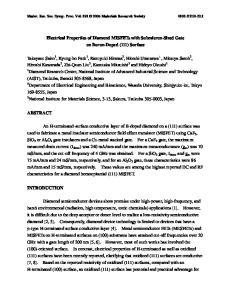
Figure 1. Cross-section of the HTD MISFET used in simulation
DEVICE STRUCTURE AND SIMULATION PARAMETERS Figure 1 illustrates the cross-section of the HTD MISFETs used in our simulation. The substrate is (001) single-crystal diamond. After hydrogenation, an ultrathin layer filled with induced acceptors is formed at diamond surface. Source/drain ohmic contacts are formed by gold evaporation, and aluminum is used to form the gate contact. The thin gate insulator (usually Al2O3) is formed during Al evaporation [10]. The device simulation is based on a standard isothermal drift-diffusion model, where the basic semiconductor equations, i.e. Poisson equation, current density equation and continuity equa
Data Loading...