Size Effects in BaTiO 3 Thin Films
- PDF / 304,940 Bytes
- 5 Pages / 414.72 x 648 pts Page_size
- 82 Downloads / 394 Views
Mat. Res. Soc. Symp. Proc. Vol. 403 01996 Materials Research Society
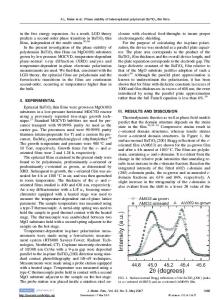
vibrating reed technique was used to measure the mechanical dissipation of the film/substrate systems. RESULTS AND DISCUSSION A. Optical Transmittance Optical transmittance of BaTiO 3 films with different grain sizes and thicknesses on fused quartz substrates was measured in the wavelength range 200-2500 nm. The grain sizes were in the range 8-35 nm and the thicknesses were in the range 1 - 8 pi m. With the increase of grain size and thickness, the absorption edge shifted to longer wavelengths, i.e. the energy gap shifted to lower energie [8]and tended to the bulk single-crystal value of 3.0 eV [9]. An increase of lattice constant was also observed with the decreasing of grain size or thickness of films. The reasons of energy gap variation may lie in: (1) the increase of lattice parameters accompanying the decrease of grain size and thickness induced the increasing of highest valance band energy and resulted in the decreasing of energy gap. The effect of lattice parameter on the energy gap in perovskite film was described elsewhere [8] (2) the more boundary atoms in the films with smaller grain size. It induced less widening of respective conduction and valence bands, and resulted in larger energy gap. (3) the deformation of crystal lattice. The deviation of lattice parameters and the deformation of crystal lattice were considered to be caused by tensile stress and its ununiform distribution. B. Raman Scattering
3000
20000 Si
2000
1. l04im 2. 84 m 3. 5ýi m
15000
5. 13im
182 306 282
10000
-
L=8L m
1000 5000 - L=8t mS5 S-lOnm
3
718
54
0 0
1 250
500
750
0
1000
Raman shift (cm 1)
0
200
400
600
800
1000
Raman shift (cm 1)
Fig. 1 Raman Spectra of BaTiO 3 films
Fig. 2 Raman Spectra of BaTiO 3 films
with different thinkness
with different grains. (10 nm, 50nm) 546
Fig. 1 shows the Raman spectra of the films with different thickness and similar grain size on Si substrates. It shows three facts: (1) The peaks become lower and broader with the decrease of film thickness. No obvious Raman peak can be seen for the films thinner than 3 p m. This phenomenon may due to less density, more lattice deformation, more defects and disorder in thinner films. (2) Three peaks displaying the characteristic of perovskite BaTiO 3 film appear for 1 the film thicker than 5 Vm. The exact position of the peaks in the vicinity of 550 cm- is difficult of frequencies of the change The to define for the peaks are overlapped by that of Si substrates. 1 1 other peaks with film thickness is shown in Table I. The modes around 300 cm- , 550 cm- , 750 1 1 cm-1 correspond to bulk materials' 270 cm-1, 520 cm- , 720 cm- modes respectively. The [10], the peak around 720 scattering Raman order higher former two were thought to belong to cm-1 might be attributed to Al and E modes. Referring to the experiments of I. Taguchi et al. [11] and K. Fujimoto [12] et al. on PbTiO 3 single crystals and BaTiO 3 thin films, and the facts that the lattice parameters of ou
Data Loading...