Size Effects of Hardness and Strain Rate Sensitivity in Amorphous Silicon Measured by Nanoindentation
- PDF / 2,833,017 Bytes
- 9 Pages / 593.972 x 792 pts Page_size
- 85 Downloads / 361 Views
use of thin films in many branches of modern industry, i.e., in photonics, micro- and nanoelectronics, and micro- and nano-electromechanical systems (MEMS and NEMS), has generated a strong interest in their mechanical properties. The requirements for mechanical reliability and durability become more crucial with increasing the complexity of the systems. Amorphous silicon (a-Si) is one of the most common materials used for manufacturing of MEMS.[1,2] In the literature, one can find evidence that processing conditions like deposition temperature, pressure, and flow rate of gases and processes like etching, chemical treatments, or ion implantation are known to affect the microstructural features as well as the distribution of volume and surface defects in this material.[3–5] To gain
DARIUSZ M. JARZA ˛ BEK is with the Institute of Fundamental Technological Research, Polish Academy of Sciences, 02-106 Warsaw, Poland and also with the Institute of Fundamental Technological Research, Polish Academy of Sciences, Pawinskiego 5B, 02-106 Warsaw, Poland. Contact e-mail: [email protected] MICHAŁ MILCZAREK and SZYMON NOSEWICZ are with the Institute of Fundamental Technological Research, Polish Academy of Sciences. PIOTR BAZARNIK is with the Warsaw University of Technology, 00-661 Warsaw, Poland. HELMUT SCHIFT is with the Paul Scherrer Institut, 5232 Villigen PSI, Switzerland. Manuscript submitted September 24, 2019.
METALLURGICAL AND MATERIALS TRANSACTIONS A
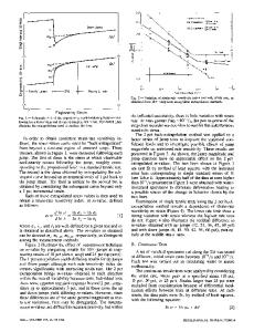
a deeper understanding between processing-structure-property-performance relationship for a-Si, much recent research interest has focused on characterizing hardness, Young’s modulus, and pressure-induced phase transformations measured, i.e., by nanoindentation.[3,5–7] This measurement method is particularly dedicated and successfully applied for studying of mechanical properties of thin films.[8–11] For example, Kiran et al. performed high-temperature nanoindentation on pure ion-implanted amorphous silicon.[5] They shown that unrelaxed a-Si deforms entirely via plastic flow, whereas a clear transition in the mode of deformation is observed in an annealed a-Si. Furthermore, Haberl et al. studied the deformation behavior of a-Si using spherical nanoindentation[7] and again observed phase transformations only in the annealed sample. It should also be noted that the phase transformation was different for different unloading rates. Furthermore, the issue of indentation-induced phase transformations in silicon has been widely studied.[12–15] Unfortunately, the problem of dependence of mechanical properties, i.e., hardness of a-Si on indentation depth or strain rate, can rarely be found in the literature. One of the parameters that indicate the dynamic behavior of the material is the strain rate sensitivity (SRS). In the literature, one can find many papers about measuring SRS of different materials with split Hopkinson bar.[16,17] On the other hand, thin films cannot be investigated with this technique. Fortunately,
the nanoindentation can also be useful for SRS determination. This techni
Data Loading...