Spectroscopic Study of Hydrogen Induced Defect in a-Ge:H
- PDF / 328,062 Bytes
- 6 Pages / 420.48 x 639 pts Page_size
- 21 Downloads / 322 Views
SPECTROSCOPIC STUDY OF HYDROGEN INDUCED DEFECT IN a-Ge:H Shu Jin 1 and Lothar Ley Institut ffir Technische Physik, Universit&t Erlangen, Erwin-Rommel-Str.1 D-8520 Erlangen, Germany
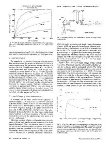
ABSTRACT Total yield photoelectron spectroscopy has been used to study the electronic structure change of UHV evaporated a-Ge subjected to posthydrogenation and various annealing cycles. We identify in R.T. hydrogenated a-Ge:H a new hydrogen induced defect at about E,, + 0.45eV, which can be healed upon 3000C annealing. This new defect accounts for the defect density gradient of hydrogenated amorphous semiconductors, spanning the range from - 10"s cm- 3 at the growing surface to 1018 - 1015 cm-3 in the bulk, depending on growth condition and time. The origin of this new defect is discussed.
INTRODUCTION Hydrogen incorporation in plasma deposition of tetrahedrally covalent amorphous semiconductors has been an interesting issue with its crucial role on electronic and structural properties. Earlier work[l, 2] showed that a-Si:H films prepapred at R.T. have a large spin defect density (-, 101s cmr- 3 ) with high hydrogen content (- 30at.%) preferentially in the form of polyhydride[3]. The origin of the defect concomitant with excess hydrogen has been unclear. Knights and Lujan attributed the degradation of films prepared at low substrate temperature to more defective morphology[4]. This attribution could not explain the experimental phenomenon that annealing around 250°C can improve R.T. deposited film to be as good as a 250°C deposited one[5, 6]. In addition, recent subgap optical absorption[7] and yield spectroscopy[8] studies indicated that the surface layer has more defects (- 3 x 10'8 cm- 3) than the bulk (3 x 1015 cm- 3 ) of a-Si:H prepared under opitimised conditions (Ts -, 250oC), while photoemission[9] and EELS[10] studies confirmed polyhydrides as dominant species in the growing surface. Therefore, more study of the correlation between defect formation and hydrogen incorporation in the growing surface will help understand the defect origin and growth process of hydrogenated amorphous semiconductors. In this study we have investigated the change in electronic structure associated with hydrogen incorporation using UHV evaporated a-Ge subjected to plasma posthydrogenation and various annealing cycles as a model system. In this way morphology change can be excluded and effects of thermal annealing and hydrogenation can be seperated.
EXPERIMENTAL DETAILS Film evaporation, posthydrogenation, yield spectrum and work function measurements were performed in three interconnected UHV chambers with a base pressure of - 10- 0 torr. a-Ge films of -, 1000A were thermally evaporated from outdegassed single crystalline Ge pieces onto polished stainless steel substrates kept at R.T.. The evaporation rate was monitored with a quartz oscillator and kept around 101/sec. The reason we choose Ge 'Present address: Dept. of Physics, Boston University, Boston, MA 02215. Mat. Res. Soc. Symp. Proc. Vol. 209. 01991 Materials Research Society
404
and not
Data Loading...