Study of Gallium-Ion-Induced Silicon Amorphization by Matching Experimental and Simulated Electron-Microscopy Images
- PDF / 701,542 Bytes
- 5 Pages / 612 x 792 pts (letter) Page_size
- 13 Downloads / 252 Views
of Gallium-Ion-Induced Silicon Amorphization by Matching Experimental and Simulated Electron-Microscopy Images A. V. Rumyantseva, *, A. S. Prikhodkoa, and N. I. Borgardta aNational
Research University of Electronic Technology—MIET, Zelenograd, Moscow, 124498 Russia *e-mail: [email protected] Received December 17, 2019; revised January 22, 2020; accepted January 24, 2020
Abstract—The atomic structure of crystalline silicon after 5-keV gallium-ion bombardment is investigated using experimental cross-sectional transmission electron microscopy imaging of the irradiated area. Atomistic molecular-dynamics simulations are performed to interpret the observed contrast. On the basis of the acquired atomic configurations, bright-field electron-microscopy images are simulated and their good correspondence with the experimental micrographs is established. To identify the structure of the material in the transition region between the crystal phase and the amorphous layer, the modulus of the sum of vectors pointing from an atom to its nearest neighbors is used. It is shown that its variations averaged over a large number of atoms are associated with the intensity distribution observed on the images. Keywords: focused ion beam, simulation of ion-surface interactions, molecular dynamics DOI: 10.1134/S1027451020050171
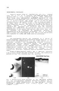
INTRODUCTION The impact of ion beams on the surface of solid samples is one of the key technological processes of modern nanotechnology. Ion bombardment is used both to change the physical properties of materials by introducing doping elements [1], and in tasks of surface nanostructuring during ion sputtering [2, 3]. Along with the introduction of impurities into the sample, ion implantation is accompanied by destruction of the crystal lattice and amorphization of the target material. In contrast to the concentration of implanted atoms, which can be determined by the methods of secondary-ion mass spectroscopy [4] or energy-dispersive X-ray microanalysis [5], finding the distribution of defects in a sample is a more challenging task. Although the amorphized region can be visualized by transmission electron microscopy (TEM) [6], further studies are required to identify the relationship between the observed contrast and defects arising from ion irradiation. Of greatest interest is prediction of the thickness of the amorphized region and the search for an adequate atomistic model of the interface between amorphous and crystalline materials. In particular, assessment of this thickness is necessary when using the focusedion-beam method (FIB) [7], which is used to fabricate nanostructures, including the preparation of samples for TEM studies [8]. To estimate the penetration depth of ions, the Monte Carlo method is usually used in the binary collision approximation. Its use in combination with the
model of the critical defect density [6] made it possible to determine the width of the amorphized layer for normal [6] and grazing beam incidence [7] with a uniformly distributed ion dose. In [9], amorphization modeling was carried out
Data Loading...