Substrates and Materials
The choice of substrate and the material requirements for GaN-based power transistors for switching applications strongly depend on the device architecture. While to date most efforts have been directed toward the fabrication of lateral devices, vertical
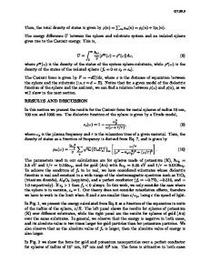
- PDF / 1,116,467 Bytes
- 26 Pages / 439.37 x 666.14 pts Page_size
- 23 Downloads / 323 Views
Substrates and Materials Stacia Keller
The choice of substrate and the material requirements for GaN-based power tran‐ sistors for switching applications strongly depend on the device architecture. While to date most efforts have been directed toward the fabrication of lateral devices, vertical device layouts have recently gained interest, catalyzed by the progress in the development of larger size bulk GaN substrates. The vertical devices have the advantage that the high fields are held within the bulk of the material rather than on the surface. Large-area GaN substrates, however, are still very expensive, making a lateral device layout on a foreign substrate such as silicon, which is available in wafer sizes up to 12″, currently more attractive. Independent of the device layout, power switching devices operate at high current densities and are required to exhibit high breakdown voltages in combination with a low on-resistance and low switching losses. Thereby, GaN-based devices take advantage of the high breakdown field, electron mobility, and saturation drift velocity of GaN, as discussed in the previous chapters of this book. At a free carrier concentration of 4 × 1016 cm−3, electron mobilities as high as 1265 cm2/Vs have been reported [1], and values of approximately 1750 cm2/Vs were extracted from I−V curves for material with a carrier concentration of about 3 × 1015 cm−3, both deter‐ mined for epitaxial layers grown on bulk GaN substrates [2]. Even higher electron mobilities can be achieved in GaN-based heterostructures, with values as high as 2200 cm2/Vs at room temperature for AlGaN/AlN/GaN heterostructures, demon‐ strated on foreign substrates [3].
S. Keller (✉) Electrical and Computer Engineering Department, University of California Santa Barbara, Santa Barbara, CA 93106, USA e-mail: [email protected] © Springer International Publishing Switzerland 2017 M. Meneghini et al. (eds.), Power GaN Devices, Power Electronics and Power Systems, DOI 10.1007/978-3-319-43199-4_2
27
28
S. Keller
Fig. 2.1 Schematics of different AlGaN/GaN transistors: a D-mode structure and E-mode structures with b recess gate or c p-(Al,Ga)N cap layer, d vertical transistor (CAVET). S source, D drain, G gate
For power switching applications, enhancement-mode (E-mode) devices are preferred, either using an intrinsic E-mode transistor or utilizing a depletion-mode (D-mode) device in a cascode arrangement [4]. D- and E-mode transistor structures can be designed using combinations of GaN with (Al,Ga)N and/or p-(Al,Ga)N layers, the growth of which will be discussed in more detail in the following sections (Fig. 2.1). While GaN-based transistors for high-frequency applications utilizing thinner GaN base layers have been fabricated by both molecular beam epitaxy (MBE) [5] and metal-organic chemical vapor deposition (MOCVD), to date transistors for power switching applications have been predominantly fabricated using the latter method, taking advantage of the higher growth rates in the MOCVD process. In addition, large-scale MOCVD reac
Data Loading...