TEM and HREM study of silicon and platinum nanoscale ensembles in 3D dielectric opal matrix
- PDF / 568,225 Bytes
- 6 Pages / 612 x 792 pts (letter) Page_size
- 90 Downloads / 254 Views
TEM and HREM study of silicon and platinum nanoscale ensembles in 3D dielectric opal matrix N. A. Feoktistov, V. G. Golubev, J.L. Hutchison1, D. A. Kurdyukov, A. B. Pevtsov, R. Schwarz2, J. Sloan3, and L.M. Sorokin Ioffe Physico-Technical Institute, RAS, 194021 St. Petersburg, Russia 1 Department of Materials, Oxford University, Parks Road, Oxford OX1 3PH, UK 2 Instituto Superior Tecnico, Departamento de Fizica, P-1096 LISBOA Codex, Portugal 3 Wolfson Catalysis Centre, Inorganic Chemistry Laboratory, Oxford University OX1 3QR UK ABSTRACT In the present paper regular systems of silicon and platinum assemblies have been fabricated in a three-dimensional (3D) void sublattice of synthetic opal. The detailed TEM and HREM structure study of ‘opal-Si’ and ‘opal-Pt-Si’ composites was carried out. It was found that in regular composites ‘opal-Si’ the silica spheres were covered uniformly with a nanocrystalline silicon layer of up to 25-30 nm in thickness. To form the Pt-Si contact the silica spheres were coated with platinum layer before embedding silicon. The results obtained demonstrate a possibility of creating 3D multilayer semiconductor structure (p-n junctions, Schottky barriers etc.) on the inner surface of opal voids. INTRODUCTION It is well known that conventional solid-state electronics is based on planar technology [1]. Three-dimensional (3D) semiconductor nanodevices are necessary for further increase of the volume density of active elements. 3D assemblies of semiconductor nanodevices can be created by using the matrix technology. Some dielectric matrices, e.g. synthetic opal possess a regular sublattice of submicron channels and voids permitting one to obtain in them 3D assemblies of nanostructures of a different type with density of elements as high as 1014 cm-3. For fabrication of silicon solid-state electronic nanodevices it is necessary to deposit homogeneous layer of given thickness on an internal surface of voids in opal matrix and to create metallic contacts. EXPERIMENTAL DETAILS ‘Crystalline’ opal consists of ordered amorphous SiO2 (silica) spheres, forming a facecentered cubic (f.c.c.) lattice [2]. Between the spheres there are voids (~26 % of a total matrix volume), which also form a regular sublattice [3]. The voids are connected to each other by means of channels. There are two types of voids: octahedral and tetrahedral. The opals are usually prepared by a method of sedimentation of synthetically grown monodispersed spherical SiO2 globules [4] obtained by a hydrolysis of tetraethoxysilane in the presence of ammonium hydroxide. The formation of submicron size spheres passes in some stages from SiO2 globules with the sizes of ~3-10 nm. Thus, inside silica spheres there is a substructure. After sedimentation the opals harden with the help of a hydrothermal annealing [3,4]. During this process most small-sized globules can be damaged and partially coagulated.
A24.4.1
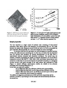
Figure 1 TEM image of annealed ‘opal-Si’ taken in diffraction contrast mode. Therefore, regular configuration inside opal spheres usually
Data Loading...