Tem/Hrem Structural Characterization of Directionally Solidified Gaas-Cras Eutectic Crystals
- PDF / 3,915,894 Bytes
- 5 Pages / 414.72 x 648 pts Page_size
- 55 Downloads / 319 Views
SOLIDIFIED GaAs-CrAs EUTECTIC CRYSTALS Sergei RUVIMOV, Zuzanna LILIENTAL-WEBER, Wendy SWIDER, and Jack WASHBURN Material Science Division, Lawrence Berkeley Laboratory, University of California, Mail Stop 62-203, 1 Cyclotron Road, Berkeley, CA 94720 Douglas E. HOLMES Electronic Materials Engineering, 829 Flynn Road, Camarillo, CA 93012
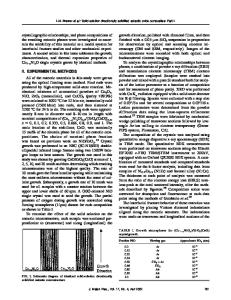
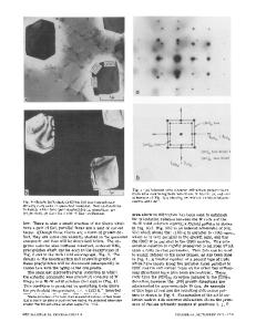
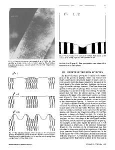
ABSTRACT Conventional and high resolution electron microscopy have been applied to characterize the microstructure of the CrAs-GaAs eutectic. The CrAs-GaAs eutectic crystals were directionally solidified by the Czochralski method in order to produce an ordered array of CrAs rods embedded in a GaAs matrix. The CrAs rods of 2-3 itm in diameter align parallel to the growth axis of the ingot. Where the GaAs matrix is found to contain structural defects, the CrAs rods are effectively defect-free. The CrAs has an orthorombic structure with the parameters a=3.5_+O.1 A, b=6.2_+0.1 A, c=5.7±0.1 A. The c-axis is close to the direction of solidification. INTRODUCTION The growth of semiconductor composites with crystallographically oriented and spacially ordered phases is a promising way to design new materials. Indeed, structures with reduced dimensionality are expected to exhibit novel physical properties. Besides a number of more conventional methods developed for fabrication of low-dimensional structures, a directional solidification approach was recently proposed to create a wire-like structure without any patterning process [1]. Although being widely used to produce metallic compositions with improved mechanical parameters [2-6], directional solidification of eutectic and off-eutectic semiconducting systems has been studied in only a few cases [7-9]. A recent study [10] of the Cr-Ga-As ternary phase diagram has identified the eutectic. However, the microstructure of the CrAs-GaAs composite has not been studied in detail. In the present work, both conventional transmission electron microscopy (TEM) and high resolution electron microscopy (HREM) have been applied to characterize the microstructure of the GaAs-CrAs eutectic directionally solidified by the Czochralski (Cz) method.
EXPERIMENTAL CrAs-GaAs samples were directionally solidified by using the high pressure liquid encapsulated Cz-method from a eutectic melt and by using a (001)-oriented GaAs seed [1]. Ingots of about 25 mm in diameter and 50 mm long were pulled at a rate of about 6 mm/hr with crystal rotation of 5 rpm. The TEMJHREM study has been carried out using Topcon 002B and ARM microscopes
151
Mat. Res. Soc. Symp. Proc. Vol. 398 01996 Materials Research Society
operated at 200 kV and 800 kV accelerating voltage, respectively. The TEM specimens were prepared by mechanical polishing followed by ion milling. The standard chemical polishing was not possible because of very different etching rates for GaAs and CrAs. Metallographic observation has been also done in addition to the electron microscopy. RESULTS AND DISCUSSION Optical micrographs of two cross sections of the ingot, perpendicular (a) and parallel (b) to the axis of
Data Loading...