The Application of Chemical Mechanical Polishing for Nickel Used in MEMS Devices
- PDF / 966,683 Bytes
- 6 Pages / 612 x 792 pts (letter) Page_size
- 103 Downloads / 291 Views
K7.5.1
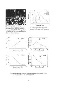
The Application of Chemical Mechanical Polishing for Nickel Used in MEMS Devices Arun Vijayakumar, Tianbao Du, Kalpathy B. Sundaram and Vimal Desai Advanced Materials Processing and Analysis Center University of Central Florida Orlando, FL 32816-2455 ABSTRACT Chemical mechanical planarization (CMP) has found extensive application in the fabrication of micro-electro-mechanical systems (MEMS). Nickel and Nickel based alloys are known to possess favorable properties that make them promising candidates to realize movable structures for MEMS applications. The development of CMP slurry chemistry for Ni that provides good CMP performance is the key in enabling CMP technology for Nickel based MEMS device fabrication. Unfortunately, very little work has been reported in terms of the electrochemical interaction of Ni with various CMP slurry constituents such as oxidizers, complexants and inhibitors. In this study, CMP of nickel was performed using H2O2 as oxidizer and alumina particles as abrasives. Electrochemical techniques were used to investigate the dissolution/passivation behavior of high-purity Ni under static and dynamic conditions in slurries at pH 4 with the addition of oxidizer, complexing agent and nickel salt. The affected surface layers of the statically etched Ni-disc were investigated using X-ray photoelectron spectroscopy (XPS). The Ni removal rate increased with the addition of oxidizer and further increased with the addition of complexing agent and nickel salt. The electrochemical results indicate that the surface chemistry and electrochemical characteristic of Ni play an important role in controlling the polishing behavior. INTRODUCTION Local and global planarization techniques have become key technologies for the fabrication of high-density integrated circuits. Chemical mechanical polishing (CMP) has emerged as the preferred manufacturing process for eliminating topographic variations and achieving waferlevel global planarization in ULSI circuits [1]. The planarization capability is an important advantage of the CMP process. It prevents problems associated with the increased number of interconnect layers in ULSI devices, where the topography of devices structures varies significantly as additional layers are stacked one on top of another. In Micro Electro-mechanical System (MEMS) applications, complex device structures are realized using the well established fabrication techniques used in the semiconductor manufacturing process. CMP processes have been developed for planarizing silicon dioxide and metal layers. Nickel and Ni based alloys have been found to have good mechanical properties that can be exploited to realize movable structures in MEMS devices, moreover the magnetic properties of Ni has been widely used in magnetic MEMS [2]. Compared to CMP for silicon dioxide, the metal (particularly nickel) CMP process is poorly understood. This is mainly due to the complex nature of electrochemical interactions between the slurry and the metal during polishing, and the coupled effect of these on the
Data Loading...