Quantitative EELS Analysis of AlGaN Nanowires Grown by Ni Promoted MBE on Sapphire Substrate
- PDF / 2,995,147 Bytes
- 6 Pages / 612 x 792 pts (letter) Page_size
- 16 Downloads / 412 Views
1026-C01-05
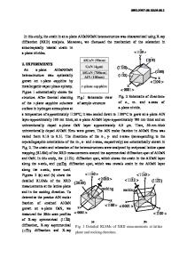
Quantitative EELS Analysis of AlGaN Nanowires Grown by Ni Promoted MBE on Sapphire Substrate Leonardo Lari1, Robert T Murray1, Mhairi H Gass2, Timothy J Bullough1, Paul R Chalker1, Caroline Chèze3,4, Lutz Geelhaar3,4, and Henning Riechert3,4 1 Dept. of Engineering, University of Liverpool, Liverpool, L69 3GH, United Kingdom 2 STFC Daresbury, SuperSTEM Laboratory, Daresbury, WA4 4AD, United Kingdom 3 Qimonda, Munich, D-81730, Germany 4 NaMLab, Dresden, D-01099, Germany ABSTRACT Quantitative analysis of the elemental distributions within AlGaN nanowires has been investigated using electron energy loss spectroscopy in a scanning transmission electron microscope. The nanowires were grown on c-sapphire by radio frequency plasma assisted molecular beam epitaxy. Crystallographic and compositional analyses of the nickel seeds used to promote the nanowire type growth yielded values of lattice spacings within the seeds remaining at the growth tip which were attributed to either (002) NiO, (111) Ni3Ga or (111) Ni-Ga solid solution. The seeds structures exhibited a metallic core encompassed by an oxide shell. The relative gallium and nickel concentrations were quantified by EELS analyses and were found to be consistent with the equilibrium phase α’ of Ni3Ga or Ni-Ga solid solution. No nitrogen was observed within the seeds, which is predicted thermodynamically due to the instability of Ni-N compounds at the NW growth temperature used in this study. No aluminium was detected at the tip of nanowires. These measurements are compared with previous studies made concerning pure GaN nanowires. The Al distribution along the nanowire length was measured and is discussed in respect of a possible Al incorporation mechanism. INTRODUCTION Within the last decade the development of GaN materials has grown dramatically as the number of potential applications has burgeoned. Optoelectronics [1] and high frequency devices [2] are just two of these applications. In particular the combination of AlN and GaN properties in heterostructures or as ternary phases (AlxGa1-xN) enlarges the bandgap making the material suitable for devices in far ultra-violet wavelength [3]. More recently, research is focused towards controlling the growth and the shape of nitride materials on nano-scale dimensions. Growth of GaN nanowires (NW) by Molecular Beam Epitaxy (MBE) has been demonstrated on sapphire and on silicon substrates, with and without the use of nickel seed as promoter of the growth [4, 5]. The next challenge is controlled growth of NW heterostructures incorporating both GaN and AlGaN. A critical issue is the control of how much aluminium is incorporated in these materials. In this paper, we report a quantitative analysis of AlGaN nanowires using electron energy loss spectroscopy (EELS) and the results are compared with previous studies made on GaN nanowires.
EXPERIMENT Radio frequency plasma assisted MBE was used to growth AlGaN nanowires on a c-axis oriented sapphire substrate modifying the growth procedure for GaN nanowires growth describ
Data Loading...