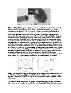
Structural Properties of Nitrides Grown by OMVPE on Sapphire Substrate
- PDF / 1,489,110 Bytes
- 10 Pages / 414.72 x 648 pts Page_size
- 41 Downloads / 329 Views
00.
7
0.09
0.91
GaN ,v-•7, 12
13
14
0T•, 15
",l,,"rF•',4 16
17
18
co [degree]
Fig. 4 X-ray rocking curve profile of (10610) diffraction from GaInN 40 nm thick on thick GaN. Molar fraction of the InN of each layer is, form the bottom, 0, 0.09, 0.21 and 1. Note that vertical scales are plotted in log scale.
483
Structural Properties of GaInN/GaN MQWs on GaN Up to now, all the LDs based on nitrides have either single quantum well or multi quantum wells structure as an active layer. Structural properties of GaInN/GaN MQWs have been characterized by the X-ray diffraction. Samples consisting of a low-temperature-deposited AIN buffer layer (30 nm), GaN layer (2 gm) and Ga1 .xIn 5N/GaN MQWs having five quantum wells, which were nominally undoped, were fabricated on the sapphire substrate by OMVPE. Thickness of the Ga1 _xlnxN well layers and the GaN barrier layers were 11 monolayers (MLs) and 22 MLs, respectively. Fig. 5 (a) shows X-ray diffraction profile of (0002) diffraction from Ga 0 821n0 18N/GaN MQW structure taken by 20/o0-scan. second order satellite peaks were clearly observed, which indicates that the interface is smooth and a well-controlled MQW was fabricated. In fig. 5 (a), calculated profiles for the different number of the GaInN MLs in the well layer based on the dynamical theory are shown. The calculated profile agrees quite well with the experimental one only when GaInN well thickness is estimated to be 11 MLs. Fig. 5 (b) also shows calculated profiles for GaInN having different InN molar fraction. The calculated profile agrees well only when the InN molar fraction is estimated to be 18 %. From these results, it is confirmed that the GaInN well layer thickness can be controlled to within one ML accuracy, the fluctuation of the alloy composition is less than 2 %, and that strain relaxation in the GaInN layer is negligibly small.
41
•
Experiments
U
CeS
U Ce U
16.0
16.5
17.0
17.5
18.0
16.0
co [degree]
16.5
17.0
17.5
18.0
co [degree]
(a)
(b)
Fig. 5 X-ray diffraction profile of five pairs of GaInN/GaN MQWs grown on GaN. Designed thickness and InN molar fraction in 11 MLs and 18%, respectively. Thickness of GaN is planned to be 22 MLs. Fig. 5 (a) shows calculated profiles for the different number of the GaInN MLs (10, 11 and 12 MLs) based on the dynamical theory. Fig. 5 (b) shows calculated profiles for GaInN having different InN molar fractions (16, 18 and 20 %).
484
Effect of Strain on The Performance of The LDs
As mentioned above, it is found that (0001)-oriented thin GaInN layers can be grown coherently on a thick GaN layer, in other words, the GaInN layers were under biaxial compressive stress. In such a case, a piezoelectric field is induced since group III nitrides have large piezoelectric constants along the [0001] orientation [30-33]. Therefore, optical properties of (0001)-oriented GaInN strained QWs should be strongly affected due to the quantumconfined Stark effect (QCSE), as are the GaInAs strained QWs grown along [111] [34-37] and the CdS/CdSe superlattice gro
Data Loading...