Quantitative Measurement of Dopant Concentration Profiling by Scanning Nonlinear Dielectric Microscopy
- PDF / 414,410 Bytes
- 6 Pages / 612 x 792 pts (letter) Page_size
- 16 Downloads / 338 Views
1025-B12-05
Quantitative Measurement of Dopant Concentration Profiling by Scanning Nonlinear Dielectric Microscopy Kenya Ishikawa1, Koichiro Honda2, and Yasuo Cho1 1
Research Institute of Electrical Communication, Tohoku University, 2-1-1 Katahira, Aoba-ku, Sendai, 980-8577, Japan 2
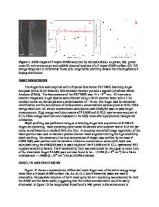
Memory Device Laboratory Fujitsu Laboratories Ltd, 10-1 Morinosato-Wakamiya, Atsugi, 243-0197, Japan ABSTRACT Using a scanning nonlinear dielectric microscopy (SNDM), we observed standard Si sample with epitaxial staircase structures, which has known dopant density values calibrated by using secondary ion mass spectroscopy (SIMS). As the result, good quantitative correlation between dopant density values and SNDM signals was obtained without the phenomenon of contrast reversal effect, which is associated with conventional scanning capacitance microscopy (SCM) measurements. Thus, it is expected that SNDM will be an effective method for observing the quantitative measurement of two-dimensional dopant profiling on semiconductor devices.
INTRODUCTION In the conventional scanning capacitance microscopy (SCM) [1-3] based dopant profiling study, it is reported and widely accepted among the SCM researchers that contrast reversal effect in the response function typically occurs at a doping level of around 1017 cm-3 in n-doped sample and around 1018 cm-3 in p-doped sample, respectively. This means met, the SCM signal level is not single-valued function against the dopant concentration. Thus, to avoid this effect and to express the relationship between SCM signal and dopant concentration as a single-valued function, DC bias application method is proposed [2, 3]. On the other hand, a scanning nonlinear dielectric microscopy (SNDM) can be used for observation of ferroelectric polarization with sub-nanometer resolution [4-6] and visualization of the charge accumulated in the flash memory [7, 8]. Recently, by applying this technique, we have succeeded in high-resolution visualizing of a dopant profile in the n-channel metal-oxide-semiconductor field-effect transistor (MOSFET) with 40 nm gate channel length between the source and drain [9].And we have demonstrated that the SNDM has much higher
performance and resolution than the SCM for observing the dopant concentration profiling, because the sensitivity to capacitance variation of SNDM is 10-22 F which is much higher than that of SCM with typical sensitivity of 10-18 F [5]. This time, as the next step of successive SNDM based dopant concentration profiling study for quantitative measurement on semiconductor devices, we observed p- and n-type Si staircase samples in air at room temperature under humidity control. To evaluate correlation between dopant concentration values and SNDM signals, the SNDM data measured without DC bias application method are compared to conventional secondary ion mass spectroscopy (SIMS) data.
EXPERIMENT The basic configuration of cantilever-type SNDM system, which is based on the atomic force microscopy (AFM), is reported previously [6-9]. An externally applied voltage
Data Loading...