Rapid thermal recrystallization of amorphous silicon films
- PDF / 367,202 Bytes
- 4 Pages / 612 x 792 pts (letter) Page_size
- 50 Downloads / 440 Views
MATERIALS RESEARCH
Welcome
Comments
Help
Rapid thermal recrystallization of amorphous silicon films G. D. Beshkov, D. B. Dimitrov, V. Lazarova, J. Koprinarova, K. Gesheva, and E. Vlaev Institute of Solid State Physics, Bulgaria Academy of Sciences, Blvd. Tzar. Chaussee 72, 1784-Sofia, Bulgaria (Received 10 January 1995; accepted 24 March 1997)
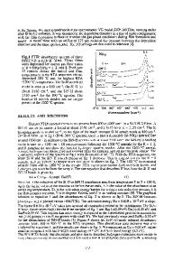
In this work the properties of polycrystalline silicon layers obtained by rapid thermal ˚ have annealing have been discussed. Amorphous silicon layers with thickness of 3000 A been deposited on silicon wafers in rf sputtering system. The layers were annealed for 15 s to 5 min at temperatures in the range 800 –1200 ±C in vacuum 5 3 1025 Torr. A correlation was established between structure, morphology, sheet resistance, and the parameters of the RTA annealing.
Amorphous and polysilicon layers are one of the commonly used elements of the modern integrated circuits and electron devices. The further development of two- and three-dimensional integrated circuits is related mainly to the properties of the silicon layers deposited on an insulator substrate.1–3 For this reason a great amount of work has been devoted to the investigation of the properties of recrystallized amorphous silicon layers performed using different apparatus and by different techniques.4–8 The present investigation has been carried out in order to establish the influence of the rapid thermal annealing temperature and the recrystallization time on the structure, morphology, and electrical properties of amorphous silicon layers deposited on silicon substrates. The application of thermally oxidized silicon wafers as a substrate for the experiments allows one to analyze the properties of the entire SOI (silicon on insulator) structure. The experiments have been carried out on n-type silicon substrates with orientation (100) and bulk resistivity of 40–62 V ? cm. The substrates have been cleaned in H2 SO4 : H2 O2y(1 : 1) for 30 min, etched in 10% HF for 10 s, and washed for 30 min in de-ionized water. After cleaning the amorphous silicon layers were deposited by rf-magnetron sputtering in the Z-400 Leybold –Heraeus system. The substrates were not intentionally heated during the deposition. The substrate temperature was of the order of 50 ±C at a sputtering current of 0.14 A and rf voltage of 1.8 kV and dc biasing of 0.27 kV with Ar supply gas. The rate of the deposition under these ˚ conditions was measured to be of the order of 75 Aymin. After the deposition the samples were annealed at high temperature for short times in vacuum. The pressure in the vacuum chamber during the annealing was 5 3 1025 Torr. The annealing has been carried out at 800 ±C, 1000 ±C, 1200 ±C, and at 1400 ±C for 15 s, 30 s, 1 min, and 5 min. The analysis of the structure and of the morphology of the annealed silicon films has been performed by the use of scanning electron microscopy J. Mater. Res., Vol. 12, No. 10, Oct 1997
http://journals.cambridge.org
Downloaded: 13 Mar 2015
(SEM) and by the use of reflection high energy electron di
Data Loading...