Rapid Thermal Oxidation of Polysilicon and Silicon
- PDF / 786,662 Bytes
- 6 Pages / 417.6 x 639 pts Page_size
- 57 Downloads / 430 Views
RAPID THERMAL OXIDATION OF POLYSILICON AND SILICON
JAIM NULMAN AG Assocaites, 1325 Borregas Ave., Sunnyvale, CA 94089
ABSTRACT Growth kinetics of silicon dioxide films grown by rapid thermal processing on polysilicon and single crystal silicon films is described. Oxides were grown in pure oxygen and oxygen with up to 4% HCI. For process time in the 1 to 120 s, oxide films thicknesses in the 2 to 36 nm are obtained with a uniformity of +2% across 100 mm wafers. These oxides show an interface density of states of 5x10 9 eV- 1cm- 2 after a 30 s post-oxidation anneal in nitrogen ambient at 1050 C. INTRODUCTION Trends in integrated circuit technology towards shrinking lateral and vertical dimensions require a reduction of the wafers thermal budget both for thickness and junction depth control. Silicon dioxide films grown by rapid thermal processing (RTP) have shown enhanced electrical and mechanical characteristics as compared to furnace grown films [1,2,3]. The enhancement is due to RTP's ability to provide very short times at temperatures above 1000 C, rapid switching of ambient gases, and single wafer processing to allow each wafer to be exposed to the same temperature-time cycle. In rapid thermal oxidation (RTO) processes, wafers are introduced into a nitrogen filled shallow quartz tube at room temperature. After a short N2 purge, pure 02 or 02 with 1 to 4% HCI is introduced to replace the N2 ambient. Then, either a one- or a two-step cycle is performed at high temperature as shown in Fig. 1. After the RTO time has elapsed, N2 is again introduced to purge out the oxidant gases. RTO processes have an advantage over furnace for the growth of gate oxides for VLSI CMOS and BI-CMOS, tunnel and interpoly oxides for EPROM and E2 PROM, and storage capacitors for Mbit dRAM technologies. In the following, growth characteristics of two-step RTO oxides on polysilicon and silicon, and its application to MOS technology are described.
a low LU
800
,,
600
1- 400
10
20
30
40
50
60
TIME (s)
Fig. 1 Wafer temperature for one- and two-step rapid thermal oxidation cycles.
Mat. Res. Soc. Syrup- Proc. Vol. 74. ý1987 Materials Research Society
642
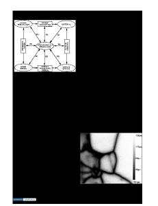
RTO OF POLYSILICON Polysilicon films with a thickness of 3000 Awere deposited by LPCVD at 620 C on silicon wafers with 20 nm thick thermally grown oxide. The polysilicon was in-situ phosphorus doped to yield a sheet resistance of about 20 ohm/sqr. Rapid thermal oxidation was performed at 950, 1050 and 1150 C in dry 02. One-step RTO processing was used in order to eliminate grain growth which would occur during the first step of two-step RTO. TEM analysis shows uniform oxide film conformal to the grains, and oxidation between grain boundaries has been avoided (Fig. 2). In contrast, with furnace processing, where large grains are formed during slow wafer loading and long temperature stabilization times. Figure 3 shows poly-oxide film thickness as function of RTO time as determined by ellipsometry. For this purpose a multiwavelength ellipsometer [4] with its wavelength set at 405 n
Data Loading...