Reconfigurable Graphene Logic Device Based on Tilted P-N Junctions
- PDF / 1,124,077 Bytes
- 12 Pages / 612 x 792 pts (letter) Page_size
- 12 Downloads / 272 Views
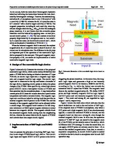
Reconfigurable Graphene Logic Device Based on Tilted P-N Junctions Sansiri Tanachutiwat, Ji Ung Lee, and Wei Wang College of Nanoscale Science and Engineering, University at Albany 257 Fuller Rd., Albany, NY 12203 USA ABSTRACT In this paper, we introduce a novel reconfigurable graphene logic based on graphene p-n junctions. In this logic device, switching is accomplished by using co-planar split gates that modulate the properties that are unique to graphene, including ambipolar conduction, electrostatic doping, and angular dependent carrier reflection. In addition, the use of these control gates can dynamically change the operation of the device, leading to reconfigurable multifunctional logic. A device model is derived from carrier transmission probability across the p-n junction for allowing quantitative comparison to CMOS logic. Based on this model, we show that the proposed graphene logic has significant advantages over CMOS gate in terms of area, delay, power, and signal restoration. Furthermore, the device utilizes a large graphene sheet with minimal patterning, allowing feasible integration with CMOS circuits, for potential CMOSgraphene hybrid circuits. INTRODUCTION Graphene, a mono-layer sheet of carbon atoms, exhibits many remarkable electronic properties. Graphene is characterized by long electron mean free path, ballistic transport, and high current density [1-6]. Its Fermi level can be tuned with a gate electrode to dope it with electrons or holes [7]. These features of graphene offer new opportunities for establishing novel carbon-based nanoelectronic systems that are functionally different from conventional CMOS devices. Several graphene nanoribbon FETs have been reported [8, 9] and these ribbons are expected to open a sufficiently large band-gap to be used as the FET channel material. However, one major challenge of using graphene ribbon is the edge scattering of the narrow ribbon, leading to relatively low mobility. Even the band gap is not well defined in these structures due to edge disorder. Therefore, it is not clear that these devices can out-perform conventional Si-based FET devices. Instead, the proposed graphene p-n junction device is based on large graphene sheets and preserves the intrinsic chiral property of carriers. Therefore, it shows a significant improvement over the nanoribbon devices by utilizing intrinsic electronic properties of large graphene sheets, and can be used to establish novel reconfigurable logic gates with high performance. Our device relies on electrostatic doping to form graded p-n junctions. The p-n junction is formed using co-planar split gates beneath a graphene sheet. The graphene sheet is laid on a very smooth surface to reduce electron scattering. By applying opposite biases (negative and positive bias voltages) to the split gates, the Fermi level of the two regions of the graphene sheet will be lowered and raised above the Dirac point, leading to p-type and n-type doping, respectively. Electrostatic doping has been used to demonstrate graphene p-n junctions [2]
Data Loading...