Reliability of Ohmic Contacts for AlGaAs/GaAs HBTs
- PDF / 2,248,049 Bytes
- 6 Pages / 420.48 x 639 pts Page_size
- 13 Downloads / 326 Views
* RELIABILITY OF OHMIC CONTACTS FOR AIGaAs/GaAs HBTs G.S. JACKSON*, E.TONG*, P.SALEDAS*, T.E. KAZIOR*, R. SPRAGUE*, R.C. BROOKS**, AND K.C. HSIEH*** *Raytheon Co., Research Div., 131 Spring St., Lexington, MA 02173
**now at:Westinghouse Electric Co., Electronic Systems Group, P.O. Box 1521, Baltimore, MD 21203 ***University of Illinois,Dept. of Elect. Eng., 1406 W.Green St., Urbana,IL61801
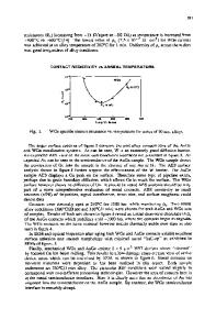
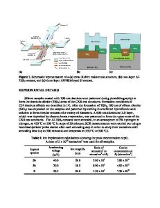
ABSTRACT The reliability of ohmic contacts to thin, heavily doped layers of GaAs isinvestigated. Pd/Ge/Au contacts to ntype GaAs display excellent electrical stability over extended periods of thermal stress. The contact resistance stays below 0.50-mim during a 2500h, 280 0 Cbake. Reactive ion beam assisted evaporation of Ti with N forms TiN which isintroduced as a barrier layer inPt/TiN/Ti/Au contacts to athin p+layer. The TiN layer allows greater process latitude inthe sintering process and improves long term stability of the ohmic contact. The microstructure of the p-type contacts isexamined with TEM and Auger profiling at different instances of the 2500h, 280 0 Cbake and compared to the contact resistance measurements. INTRODUCTION Reliability of heterostructure bipolar transistor (HBT) devices and of the fabrication process depends critically upon the ohmic contacts. Inparticular the base contact isplaced on avery thin (-1000A) heavily doped layer. A reliable process requires broad process latitude allowing optimization of contact formation, including the alloying or sintering cycle, without shorting the underlying p-n junction beneath the base contact. The issue of long term reliability under the fields and temperatures associated with device operation isrelated. Both involve interdiffusion of the contact metallurgy and the underlying semiconductor. We report the development of ohmic contacts which simplify the HBT process techniques and exhibit good aging qualities. The contacts must exhibit low resistance and maintain this property for long periods. Preferably the same sintering conditions for both n-and p-type contacts will be used. For n-type contacts Pd/Ge/Au exhibits low contact resistance and excellent long term stability for FETs [1]. This metallurgy has been chosen for the n-type contacts. For ptype contacts the use of TiN as a diffusion barrier ina Pt/barrier layer/Au sandwich isinvestigated [21. The TiN isdeposited by reactive ion beam assisted evaporation (RIBAE). Thus itiscompatible with a photoresist lift-off process utilizing electron-beam evaporation [3]. EXPERIMENT Three wafers, which duplicate the base and collector layers of an emitter-up HBT, are processed. The structure, grown by MBE on semi-insulating GaAs, is5000A of n+GaAs (3x10 18 cm' 3), 5000A of n GaAs (5x10¹⁶ cmA), finishing with 1000A 0+ GaAs (5x10 19 cm' 3 ). The n-type dopant is Si and the p-type dopant isBe. The process sequence starts with a mesa etch to isolate the devices, acollector recess etch to the n+ layer and metallization, and finally base metallization on the p+GaAs. The photolithography patterns includes atransmission line model
Data Loading...