Residual Stress Generation During Constrained Sintering of Layered Ceramic Thin Film Structures
- PDF / 1,568,531 Bytes
- 6 Pages / 414.72 x 648 pts Page_size
- 34 Downloads / 308 Views
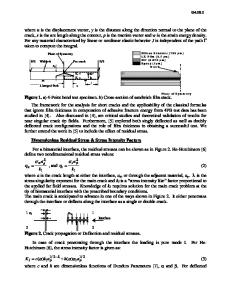
cracking, interface delamination or undesirable distortion of the component upon cooling[1]. Traditionally, sintering conditions for layered ceramic structures have been optimised by trial and error. This is time consuming, often unreliable, and results in a long product development cycle. Furthermore, prediction of the microstructural features resulting from sintering under a different set of processing conditions is not possible. In this work these issues are addressed by extending an existing constitutive formulation to deal with the nonisothermal conditions typical of many thin film processes involving sintering. First, the sintering kinetics of layered ceramic structures used in the fabrication of planar solid oxide fuel cells is investigated experimentally. The constitutive formulation is then introduced and applied to describe the evolution of the microstructural variables (i.e. relative density and mean grain size) and stresses developed during sintering and subsequent cooling. EXPERIMENTS Sintering Conditions A 200 prm thick pre-sintered yttria-stabilised zirconia (YSZ) sheet was used as the rigid substrate. A 50 pm thick film of a commercial cathode powder, viz. Lao.85Sr0.1 5 Mnl.1003, with an average particle size of 1 pm was applied on the YSZ electrolyte by multiple screenprinting. The time vs. temperature profiles used in the sintering experiments are shown in 547
Mat. Res. Soc. Symp. Proc. Vol. 505 0 1998 Materials Research Society
Fig. 1. Here, the peak sintering Tenp
temperatures
and corresponding
dwell times are identified in each
curve. A 2°C/min heating / cooling rate was used throughout. At least two 25mm square samples were the
6 nIin
1200
1300°C 60rnin.
1000 o\"
1300°C'0mn
After
800
resultant
600
sintered at each condition. sintering,
(0C) -1/00
1300oC, 30 min
12000C,0
microstructures were studied under a JOEL JSM 5300 SEM with image grabbing capabilities. Due
4W--
to the highly porous nature of the
200 -
sintered films and difficulties in polishing, the level of porosity and
0
average grain size were determined
". ll00T, 0mi~n. "
0
200
400
600
800
1000
1200
1400
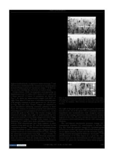
Tm(min) from direct observations of the Fig. 1 Heating and cooling profiles of sintering film surface. At least two images experiments taken from randomly selected areas were analysed in each case. Further experimental details are reported elsewhere [2][3]. Observed Microstructural Features SEM micrographs of the as-received (i.e., green) cathode showed particles of irregular shape with a wide spread of particle (< 5 pm) and pore (
Data Loading...